Apparatus and method for sensing electromagnetic radiation using a tunable device

a technology of electromagnetic radiation and bolometer, which is applied in the field of sensing devices, can solve the problems of inability to detect the specific frequency or spectral composition of the incoming infrared radiation, and limitations of conventional bolometer devices, and achieves the effects of improving performance, convenient use, and high device yield per wafer

Inactive Publication Date: 2005-01-27
CALIFORNIA INST OF TECH +1
View PDF8 Cites 60 Cited by
  • Summary
  • Abstract
  • Description
  • Claims
  • Application Information

AI Technical Summary

Benefits of technology

Many benefits are achieved by way of the present invention over conventional techniques. For example, the present technique provides an easy to use process that relies upon conventional technology. In some embodiments, the method provides higher device yields in dies per wafer. Additionally, the method provides a process that is compatible with conventional process technology without substantial modifications to conventional equipment and processes. Preferably, the invention provides for a method and device that can provide selective defection of certain IR frequencies. ...

Problems solved by technology

Accordingly, limitations exist with such conventional bolometer devices.
That is, these devices ...

Method used


Image

  • Apparatus and method for sensing electromagnetic radiation using a tunable device
  • Apparatus and method for sensing electromagnetic radiation using a tunable device
  • Apparatus and method for sensing electromagnetic radiation using a tunable device

Examples


examples

To illustrate certain principles and operations of the present invention, we have proposed certain experiments and prepared designs to carryout the functionality of certain aspects of the invention defined herein. As will be appreciated, these experiments are merely examples, which should not unduly limit the scope of the claims herein. One of ordinary skill in the art would recognize many variations, modifications, and alternatives. Also, the experiments and designs described herein are merely intended to assist the reading in understanding certain aspects of the invention without limiting the claims as recited herein.

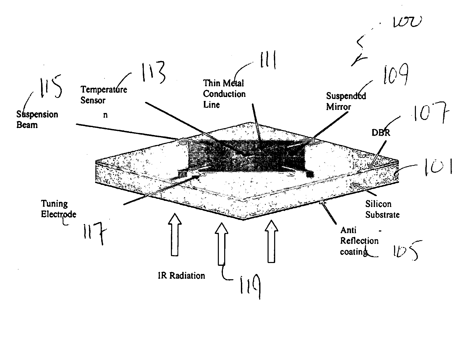
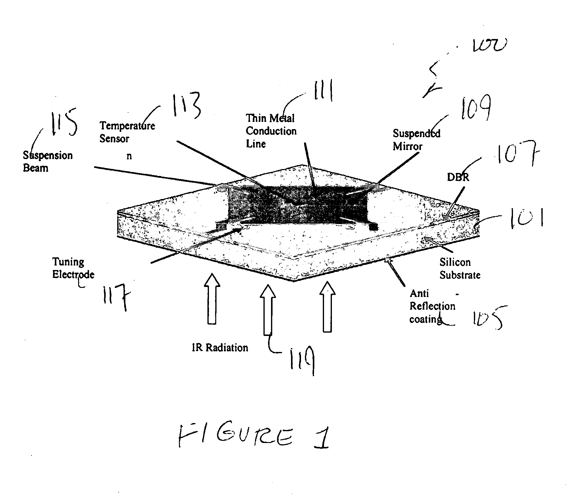
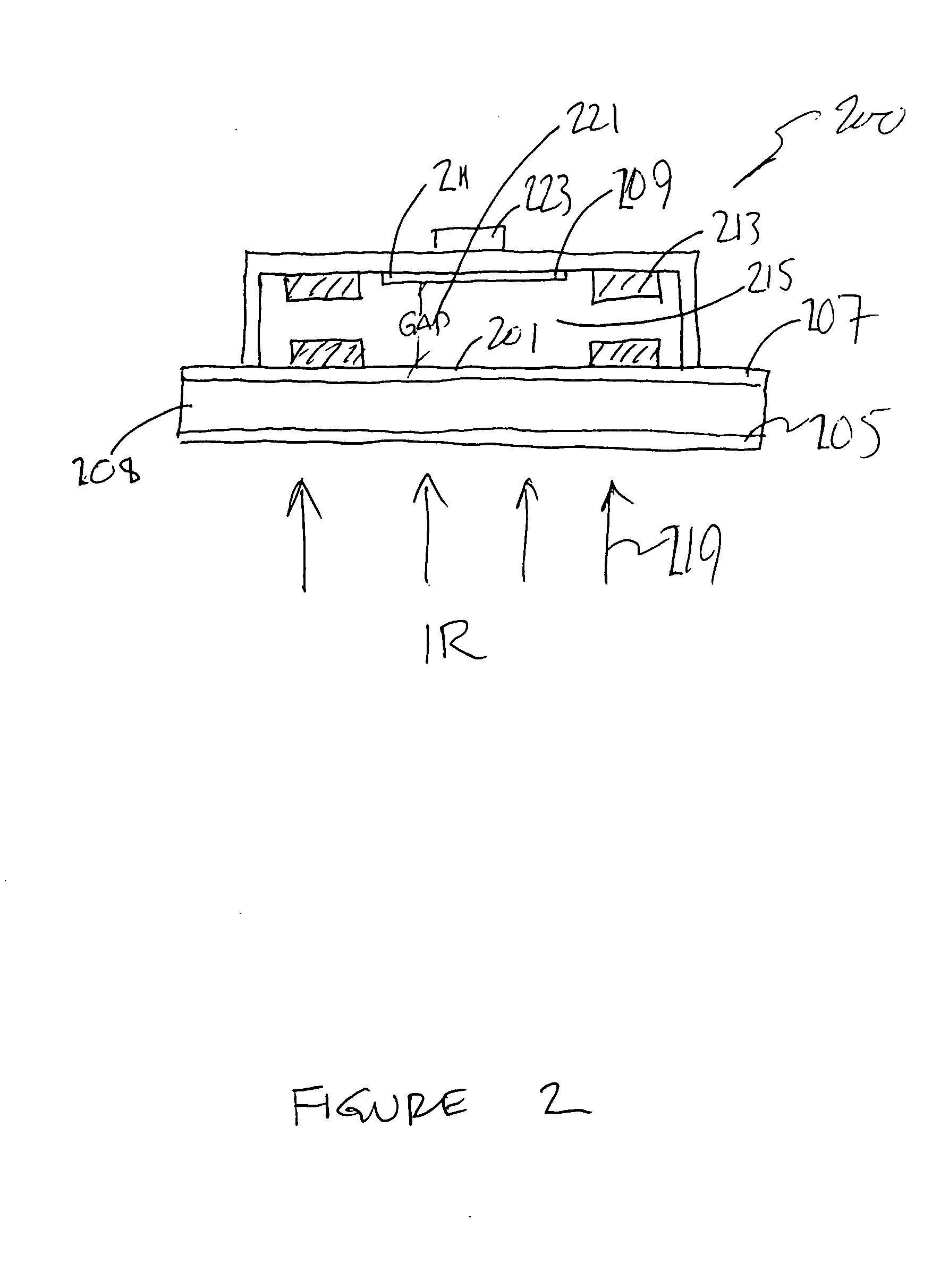
We have proposed a resonance-enhanced intra-cavity tunable bolometer design that enables high absorption (e.g., >90%), high resolution (e.g., FWHM <0.03 μm at LWIR), low noise (e.g., NETD as low as 6 mK), high speed (e.g., 60 Hz frame rate and greater), and broad tuning range (across LWIR). Of course, there can be other variations, modifications, and alternati...


PUM


Abstract

A method for manufacturing a sensing device, such as a bolometer device or other devices. The method includes providing a substrate, e.g., silicon wafer. The method includes forming a first reflection layer overlying the substrate and forming a first electrode layer overlying the substrate. The method includes forming a sacrificial layer overlying a portion of the first reflection layer and a portion of the first electrode layer. The sacrificial layer is patterned using photolithography techniques. The patterned sacrificial layer corresponds to a cavity region. The method also forms a second electrode layer overlying the sacrificial layer and forms an elastic layer overlying the patterned sacrificial layer. The elastic layer encloses the cavity region corresponding to the patterned sacrificial layer. The method releases the sacrificial layer to form an opening in the cavity region.

Description

BACKGROUND OF THE INVENTION The present invention is directed to sensing devices and their processing. More particularly, the invention provides a method and apparatus for sensing electromagnetic radiation in the infrared spectrum using a tunable bolometer device. But it would be recognized that the invention has a much broader range of applicability. For example, the invention can be applied to other wavelengths such as millimeter waves or visible light and others. As technology progresses, detection devices have become important. Detection devices range from motion sensors to those that detect certain frequencies of electromagnetic radiation. Such detection devices include, among others, infrared detectors and imagers. As merely an example, conventional infrared detectors, commonly known as bolometers, received interest from their ability to detect infrared radiation through changes in temperature. Preferably, such bolometers work at room temperature, but can also work at other ...

Claims


Application Information

Patent Timeline
IPC IPC(8): G01J3/26G01J5/20
CPCG01J3/26G02B26/001G01J5/20
Inventor TAI, YU-CHONGLIGER, MATTHLEUWU, MINGTSAI, JUI-CHE
Owner CALIFORNIA INST OF TECH
Why Eureka
Try Eureka