Thickness Estimation Using Conductively Related Calibration Samples

a technology of conductive films and calibration samples, applied in the field of eddy current measuring systems, can solve the problems of sensor sensitive to errors, destructive, non-destructive,

Inactive Publication Date: 2005-01-27
LE CUONG DUY
View PDF25 Cites 37 Cited by
  • Summary
  • Abstract
  • Description
  • Claims
  • Application Information

AI Technical Summary

Problems solved by technology

These inspection procedures include destructive, as well as nondestructive, testing methods for analyzing wafer products.
However, measuring accuracy usually begins to degrade as the coating thickness falls below the 10,000 Å threshold.
Although eddy current sensors provide highly accurate readings, these sensors are susceptible to error.
For example, the shifting of an electronic reference point due to thermal drifting often occurs at some point during the data collection and inspection process.

Method used


Image

  • Thickness Estimation Using Conductively Related Calibration Samples
  • Thickness Estimation Using Conductively Related Calibration Samples
  • Thickness Estimation Using Conductively Related Calibration Samples

Examples


Embodiment Construction

In the following description of preferred embodiments, reference is made to the accompanying drawings, which form a part hereof, and which show by way of illustration, specific embodiments of the invention. It is to be understood by those of ordinary skill in this technological field that other embodiments may be utilized, and structural, electrical, as well as procedural changes may be made without departing from the scope of the present invention.

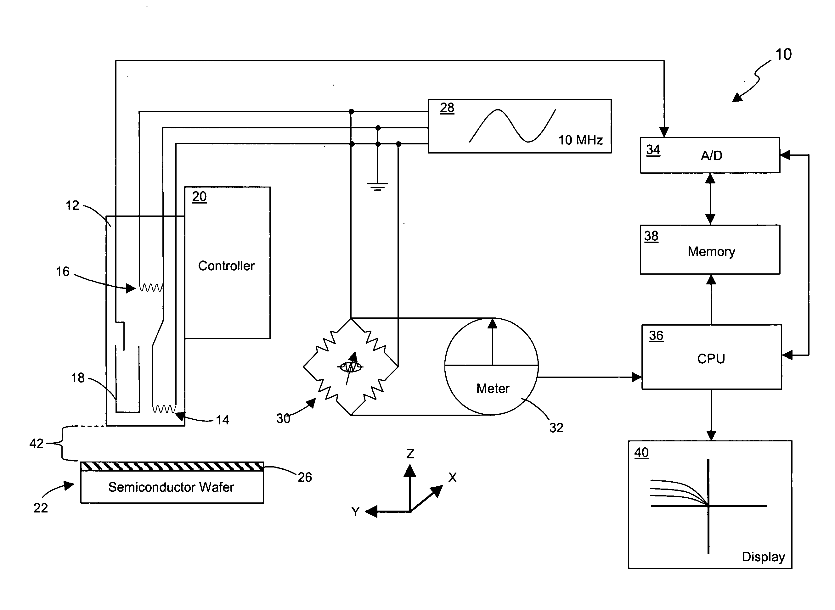
FIG. 1 is a diagram showing a single-probe eddy current measuring system 10 in accordance with some embodiments of the present invention. As shown, the system includes a conventionally configured eddy current probe 12 having sense coil 14, reference coil 16, and capacitance sensor 18. The eddy current probe is shown in communication with controller 20, which, during operation, may provide relative motion between the eddy current probe and substrate 22. In a typical implementation, the controller translates the eddy current probe and inc...


PUM

PropertyMeasurementUnit
frequencyaaaaaaaaaa
resistanceaaaaaaaaaa
distanceaaaaaaaaaa

Abstract

A method for monitoring an inspection sample includes generating inspection data comprising resistance and reactance measurements that are obtained from an inspection sample having a conductive layer of unknown thickness. Calibration data is used for estimating the thickness of the conductive layer of the inspection sample. This calibration data includes resistance and reactance measurements obtained from one or more calibration samples, each calibration sample having a conductive layer of known thickness. The conductive layers of the inspection sample and the calibration samples comprise different materials having a known conductive relationship.

Description

BACKGROUND OF THE INVENTION 1. Field of the Invention The present invention relates generally to an eddy current measuring system, and in particular to an eddy current measuring system for estimating the thickness of conductive films formed on semiconductor wafer products. 2. Description of the Related Art In the semiconductor industry, critical steps in the production of semiconductor wafers are the selective formation and removal of films on an underlying substrate. The films are made from a variety of substances, and can be conductive (for example, metal or a magnetic ferrous conductive material) or non-conductive (for example, an insulator or a magnetic ferrite insulating material). Films are used in typical semiconductor processing by: (1) depositing a film; (2) patterning areas of the film using lithography and etching; (3) depositing material which fills the etched areas; and (4) planarizing the structure by etching or chemical-mechanical polishing (CMP). Films may be fo...

Claims


Application Information

Patent Timeline
Patent Type & Authority Applications(United States)
IPC IPC(8): B24B49/00G01B7/06G01N27/72G01R33/12
CPCG01B7/105
Inventor LE, CUONG DUY
Owner LE CUONG DUY
Why Eureka
Try Eureka