Method for forming flowable dielectric layer in semiconductor device
- Summary
- Abstract
- Description
- Claims
- Application Information
AI Technical Summary
Problems solved by technology
Method used
Image

Examples
Embodiment Construction
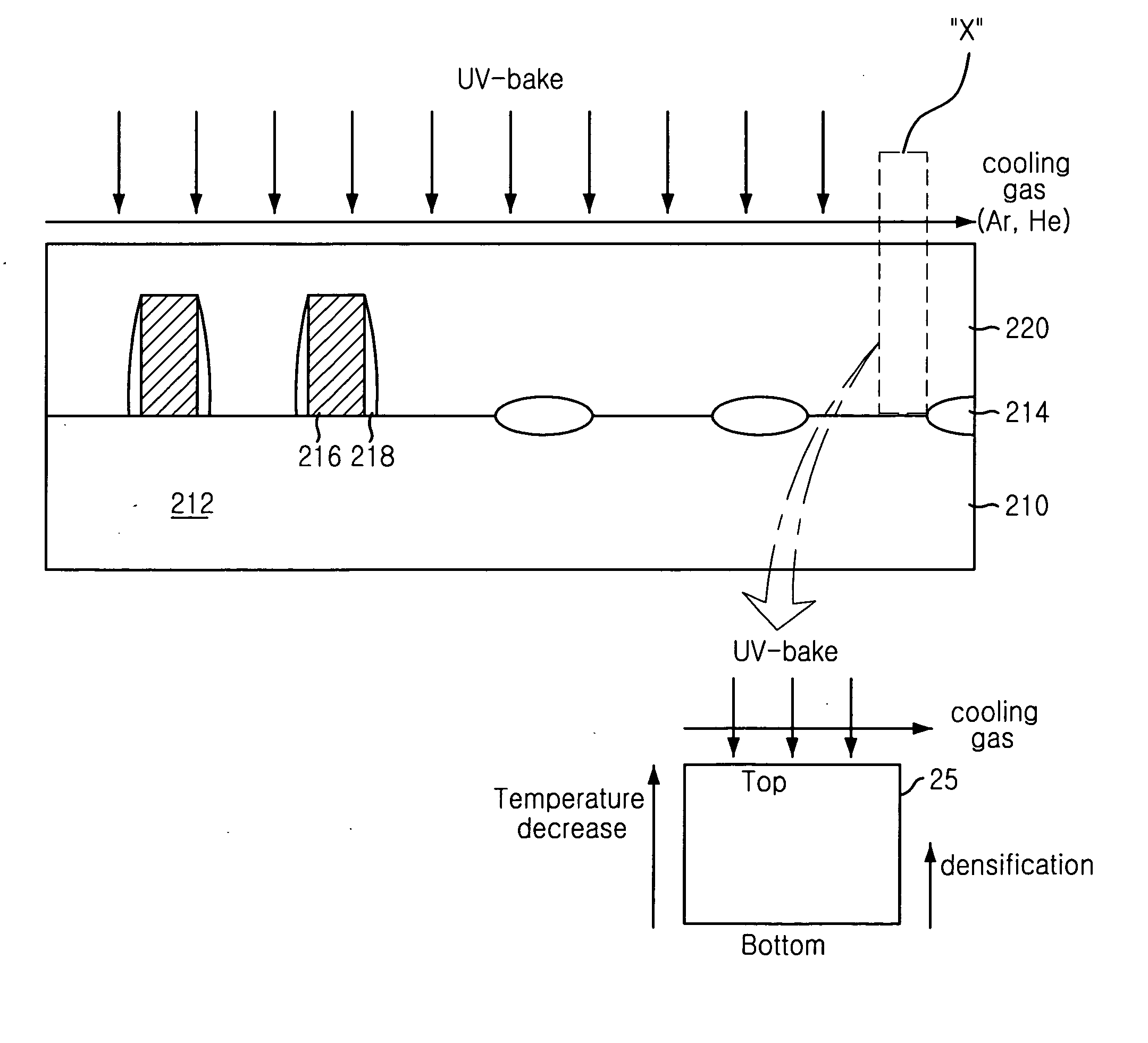
[0022] There are provided in FIGS. 3A to 3D cross sectional views setting forth a method for forming a flowable dielectric layer in a semiconductor device in accordance with a preferred embodiment of the present invention.
[0023] In FIG. 3A, an inventive method begins with preparing a semiconductor substrate 210 where field oxide (FOX) areas 214 and an active area 212 are defined in preset locations of the semiconductor substrate 210 by a predetermined process. Thereafter, gates 216 are formed on predetermined locations of a top face of the semiconductor substrate 210, wherein there is formed a gap between adjacent gates 216 having a narrow space. Afterward, sidewall spacers 218 are formed on sidewalls of the gates 216 by using a typical etching process in which the sidewall spacers 218 uses a silicon nitride. As is well known, there are typically formed gate oxides (not shown) beneath the gates 216 and the gates 216 may be a stack structure of a polysilicon layer, a metal layer and...
PUM
 Abstract
Description
Claims
Application Information
 - R&D Engineer
- R&D Manager
- IP Professional
- Industry Leading Data Capabilities
- Powerful AI technology
- Patent DNA Extraction
Browse by: Latest US Patents, China's latest patents, Technical Efficacy Thesaurus, Application Domain, Technology Topic.
© 2024 PatSnap. All rights reserved.Legal|Privacy policy|Modern Slavery Act Transparency Statement|Sitemap