System and method for performing design verification

a verification system and design technology, applied in the field of design verification systems, can solve the problems of inconvenient verification of electronic systems, and inability to perform instruction set simulators, etc., to achieve the effect of facilitating communication among system elements, ensuring portability and flexibility, and facilitating verification of electronic systems

Active Publication Date: 2005-01-27
CADENCE DESIGN SYST INC
View PDF3 Cites 30 Cited by
  • Summary
  • Abstract
  • Description
  • Claims
  • Application Information

AI Technical Summary

Benefits of technology

[0011] Since one or more of the system elements may be provided on an incompatible development platform, each system element is provided with a co-verification interface to facilitate communications among the system elements. The co-verification interfaces couple the system elements with the communication system and preferably is provided as a layered protocol stack to assure portability and flexibility. The system elements exchange communication signals via the communication system to execute the overall design verification system and to provide debugging services. Since the hardware development platforms can be configured to provide an operating system for the virtual elements, a number of clock cycles expended during interactions among the physical elements and the virtual elements can be reduced such that verification of the electronic system can be performed more quickly.
[0012] Considerable debugging of the electronic system can be achieved while the virtual elements remain in their virtual form. Once the electronic system is stable, one or more of the virtual elements can be refined to a register transfer level (RTL) form for further testing. The virtual elements subsequently can be compiled into a field programmable gate array (FPGA) for more extensive verification at full speed. As each virtual element is converted to a physical form, system performance and verification coverage increase.

Problems solved by technology

Since silicon turns (each “silicon turn” is a complete fabrication of chip) can account for a large portion of the total cost and time for developing a system-on-chip, considerable hardware verification is performed prior to fabrication.
With current designs, presently available simulators and workstations have proven unsatisfactory because performance of such models ranges between approximately one and one thousand cycles per second, which is inadequate for operating the software components.
This is an improvement over the event driven simulators discussed above, but instruction-level instruction set simulators also have substantial limitations.
Instruction set simulators, for instance, are not useful when cycle level accuracy is needed to model software execution speed, which often is necessary in media processing systems and other real-time embedded systems.
A fully accurate cycle level instruction set simulator, which employs accurate models of internal pipelines, speculative execution, and cache and memory management unit (MMU) behavior, is very difficult to design.
Further, since the central processing unit's cache and / or memory management unit typically are not modeled, instruction set simulators do not present the same sequence of transactions to both the modeled hardware components and physical hardware components.
The use of field programmable gate arrays however is limited to small, modular hardware components, while hardware assisted accelerators require custom processors, which can be expensive.
However, the new components, once in synthesizable register transfer level form, are difficult to debug and revise, resulting in increased cost and longer development times.

Method used


Image

  • System and method for performing design verification
  • System and method for performing design verification
  • System and method for performing design verification

Examples


Embodiment Construction

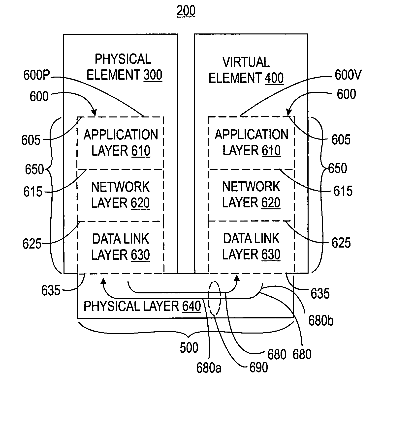
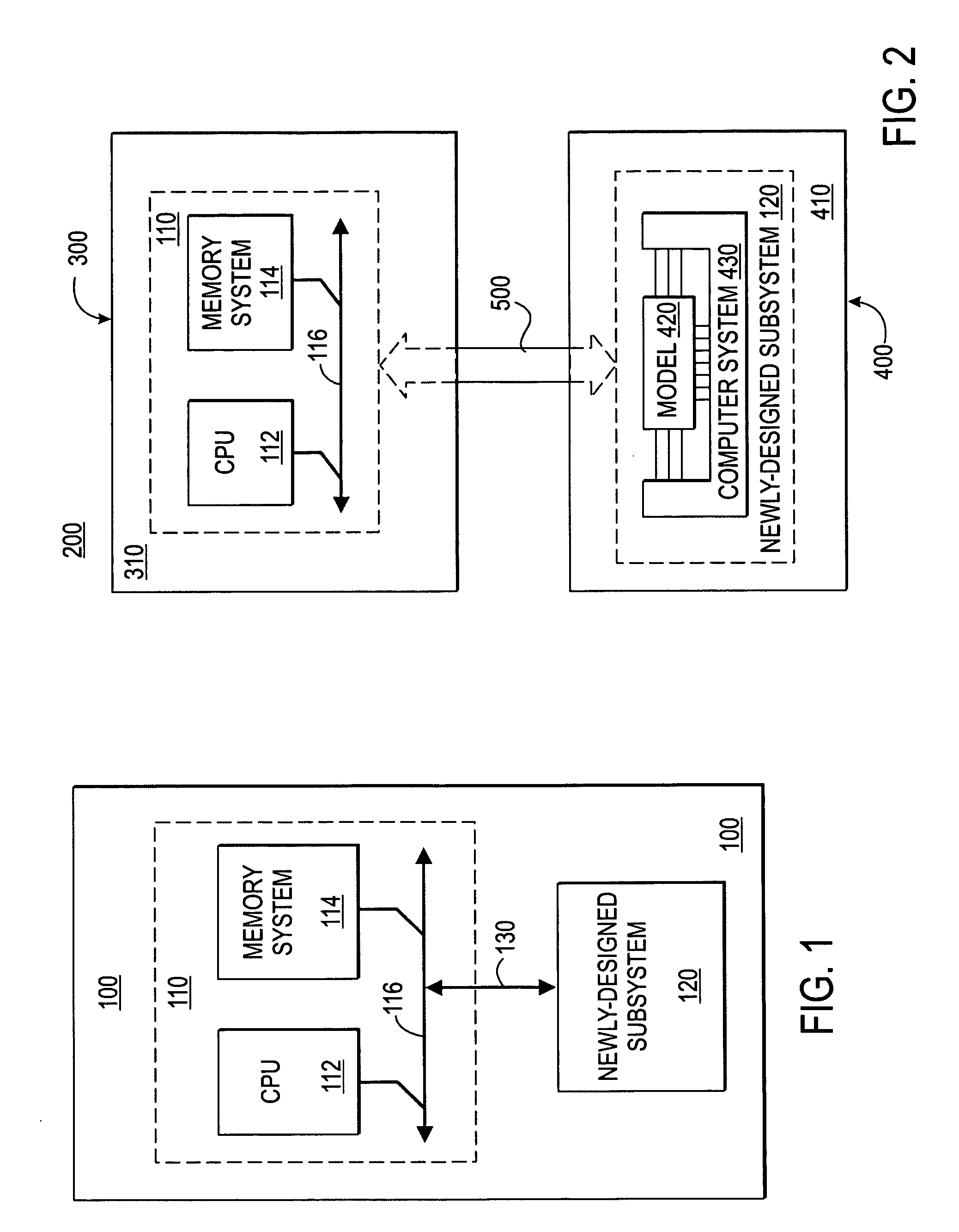
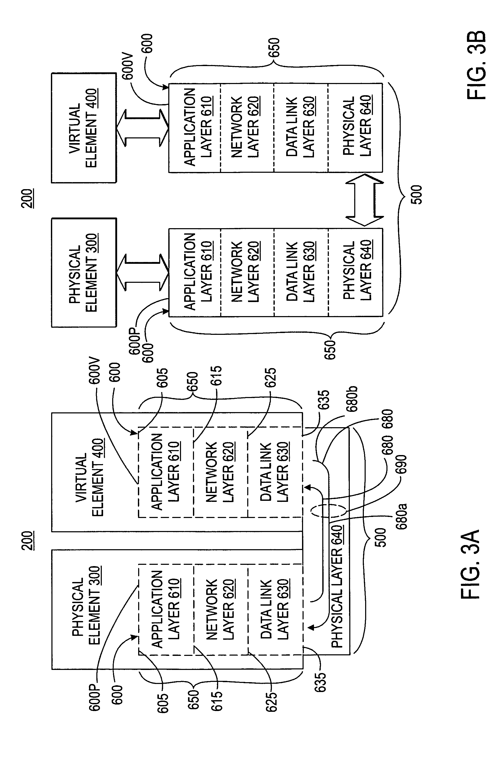
[0021] Since current design verification systems require highly accurate component modeling and can prove difficult and costly to implement, a design verification system that provides a flexible interface and protocol for interconnecting and co-verifying physical and virtual elements of an electronic system under development can prove much more desirable and provide a basis for a wide range of electronic applications, such as the development of system-on-chip (SoC) modules. This result can be achieved, according to one embodiment disclosed herein, by employing a design verification system 200 (shown in FIG. 2).

[0022] Turning to FIG. 1, the development of an electronic system 100 normally involves an integration of one or more subsystems, including existing subsystems 110, newly-designed subsystems 120, or both. Although the electronic system 100 can comprise a new, but untested, combination of existing subsystems 110, a more typical electronic system 100 includes at least one newly...


PUM


Abstract

A design verification system for developing electronic systems and methods for manufacturing and using same. The design verification system comprises a plurality of system elements, including at least one physical (or hardware) element and/or at least one virtual (or software) element, which are coupled, and configured to communicate, via a general communication system. Since the system elements may be provided on dissimilar development platforms, each system element is coupled with the communication system via a co-verification interface, which is provided as a layered protocol stack to assure portability and flexibility. Through use of the co-verification interface, the design verification system can be configured to support a wide variety of mixed physical/virtual systems.

Description

FIELD OF THE INVENTION [0001] The present invention relates generally to design verification systems and more particularly, but not exclusively, to design verification systems for developing system-on-chip (SoC) modules. BACKGROUND OF THE INVENTION [0002] System-on-chip (SoC) technology presents a major revolution in the design of integrated circuits because of the unprecedented levels of integration possible. A system-on-chip has both hardware and software components. The hardware components can include one or more central processing units (CPUs), memory systems, special functions devices, buses, and interfaces; whereas, operating systems, applications, and drivers are exemplary software components. [0003] Because the hardware components execute the software components, these hardware and software components are dependant on each other. Despite this, the hardware and software components typically are separately developed, often by different people. Since silicon turns (each “silico...

Claims


Application Information

Patent Timeline
Patent Type & Authority Applications(United States)
IPC IPC(8): G06F9/45G06F17/50
CPCG06F17/5022G06F30/33
Inventor BUTTS, MICHAEL R.MEDNICK, ELLIOT H.
Owner CADENCE DESIGN SYST INC
Why Eureka
Try Eureka