Booster circuit

a technology of boosting circuit and boosting voltage, which is applied in the direction of electric variable regulation, process and machine control, instruments, etc., can solve the problems of large circuit scale, difficult control of boosted output potential, delay in determining output potential, etc., and achieve the reduction of boosting ability, preventing overshoot of boosted voltage, and reducing power supply current in the operation of boosting section.

Active Publication Date: 2005-02-03
NORTH PLATE SEMICON LLC
View PDF6 Cites 26 Cited by
  • Summary
  • Abstract
  • Description
  • Claims
  • Application Information

AI Technical Summary

Benefits of technology

[0022] In the fourth booster circuit, delays are applied to the plurality of charge transfer transistors to gradually increase the number of operating charge transfer transistors. Accordingly, even with such a simple circuit configuration, the peak value of power supply current in operation of the boosting section is reduced.
[0023] The first through third booster circuits preferably further include a boosted voltage detection control section for detecting the output voltage from the boosting section and outputting the control signal. Then, the boosting ability is reduced as the boosted voltage approaches a target voltage value. As a result, overshoot of the boosted voltage is prevented.
[0024] In this case, the booster circuits preferably further include a power supply voltage detection control section for detecting a power supply voltage and controlling the output of the boosted voltage detection control section. Then, the boosting ability is adjusted in accordance with the power supply voltage, so that the boosting ability is not reduced too much in operation at a low power supply voltage. Accordingly, overshoot of the boosted voltage is prevented even if a power supply voltage with a relatively wide bandwidth (range) is boosted. In addition, a delay in a setup time at a low-power-supply-voltage side is prevented.
[0025] The first through third booster circuits preferably further include a boosted voltage detection control section for detecting a power supply voltage and outputting the control signal. Then, the boosting ability is not enhanced too much even if the power supply voltage is high. Accordingly, even if a power supply voltage with a relatively wide bandwidth is boosted, overshoot of the boosted voltage is prevented.

Problems solved by technology

However, in the booster circuit shown in FIG. 20, overshoot or undershoot occurs in the output potential with respect to a given boosted potential, i.e., a target value, as shown in FIG. 21, so that it is difficult to control the boosted output potential.
This is because the booster circuit is switched between boosting operation and boosting suspension in accordance with the output potential, so that a sense delay and other factors cause a delay in determining the output potential.
The conventional boosting technique for controlling the pumping pulse width has another problem of large circuit scale and a large amount of power consumption in a control circuit for controlling the pulse width.
This problem arises because the pulse-width control circuit controls the pulse width by generating an intermediate potential in accordance with the output value of the boosted potential and inputting the intermediate potential to a pulse generator.

Method used


Image

  • Booster circuit
  • Booster circuit
  • Booster circuit

Examples


embodiment 1

[0049] (EMBODIMENT 1)

[0050] A first embodiment of the present invention will be described with reference to the drawings.

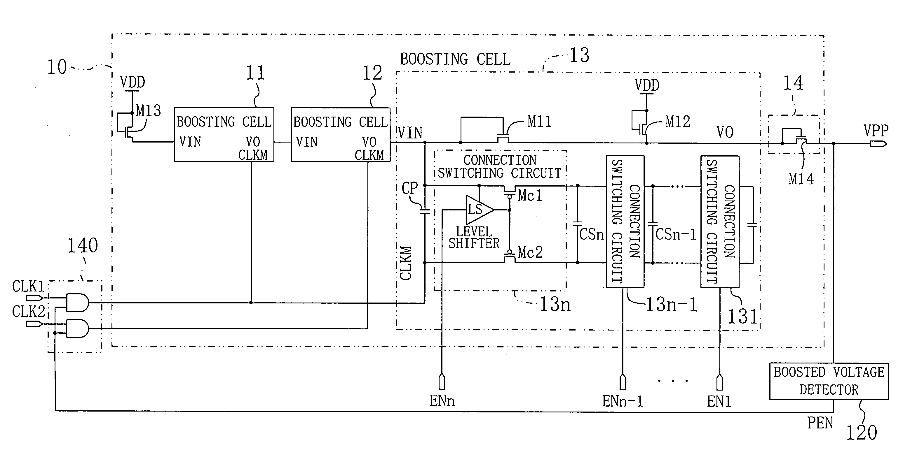
[0051]FIG. 1 shows a booster circuit according to the first embodiment of the present invention.

[0052] As shown in FIG. 1, the booster circuit of the first embodiment includes: a boosting section 10 including boosting cells 11, 12 and 13 in three stages connected in series and a power outputting unit 14 which is provided at the output side of the boosting cell 13 at the final stage and is constituted by an n-transistor M14 having a diode connection; a boosted voltage detector 120 for detecting an output voltage (boosted voltage) VPP output from the boosting section 10 and, when the detected output voltage VPP is lower than or equal to a given voltage value, outputting a clock control signal (detection signal) PEN; and a boosting clock control circuit 140 for selectively outputting a clock signal CLK1 or CLK2 received from the outside to each of the boosting cell...

embodiment 2

[0068] (EMBODIMENT 2)

[0069] Hereinafter, a second embodiment of the present invention will be described with reference to the drawings.

[0070]FIG. 4 shows a booster circuit according to the second embodiment of the present invention. In FIG. 4, each member already shown in FIG. 1 will be identified by the same reference numeral, and the description thereof will be omitted.

[0071] As shown in FIG. 4, the booster circuit of the second embodiment includes: a boosting section 10A including boosting cells 21, 22 and 23 in three stages connected in series and a power outputting unit 24 provided at the output side of the boosting cell 23 at the final stage and constituted by an n-transistor having a diode connection; a boosted voltage detector 120 for detecting an output voltage (boosted voltage) VPP output from the boosting section 10A and, when the detected output voltage VPP is lower than or equal to a given voltage value, outputting a clock control signal PEN; a boosting clock control ...

embodiment 3

[0082] (EMBODIMENT 3)

[0083] Hereinafter, a third embodiment of the present invention will be described with reference to the drawings.

[0084]FIG. 6 shows a booster circuit according to the third embodiment of the present invention. In FIG. 6, each member already shown in FIG. 1 will be identified by the same reference numeral, and the description thereof will be omitted.

[0085] As shown in FIG. 6, the booster circuit of the third embodiment includes: a boosting section 10B including boosting cells 31, 32 and 33 in three stages connected in series and a power outputting unit 34 which is provided at the output side of the boosting cell 33 at the final stage and is constituted by an n-transistor having a diode connection; a boosted voltage detector 120 for detecting an output voltage (boosted voltage) VPP output from the boosting section 10B and, when the detected output voltage VPP is lower than or equal to a given voltage value, outputting a clock control signal PEN; and a boosting c...


PUM


Abstract

Each boosting cell includes: a first n-transistor having a diode connection; a second n-transistor whose gate and drain are connected to a power supply voltage and whose source is connected to the source of the first n-transistor; and a boosting capacitor provided between the drain of the first n-transistor and a boosting clock input terminal to which a clock signal is input. The boosting capacitor is connected to n auxiliary boosting capacitors in parallel via connection switching circuits controlled with boosting ability switching signals as control signals input from the outside.

Description

BACKGROUND OF THE INVENTION [0001] The present invention relates to booster circuits for use in semiconductor integrated circuit devices such as nonvolatile semiconductor memories. [0002] A booster circuit that compares an increased output potential (boosted potential) with a reference potential to control the upper limit of the boosted potential has been conventionally used to prevent the breakdown of a transistor provided to determine the upper limit of the boosted potential in a high-voltage supplying circuit for erasing and writing in a nonvolatile semiconductor memory, for example, (e.g., in Japanese Laid-Open Publication No. 4-132088). [0003]FIG. 20 shows an example of a configuration of a conventional booster circuit disclosed in the above publication. [0004] As shown in FIG. 20, each of n pumping circuits 811 through 81n (where n is an integer of one or more) includes: first and second nMOS transistors MN1 and MN2 which are connected in series and each of which has its gate ...

Claims


Application Information

Patent Timeline
Patent Type & Authority Applications(United States)
IPC IPC(8): G11C16/06H01L21/822H01L27/04H02M3/07
CPCH02M3/073
Inventor SUWA, HITOSHIHAMAMOTO, YUKIMASA
Owner NORTH PLATE SEMICON LLC
Why Eureka
Try Eureka