
Apparatus for reducing data corruption in a non-volatile memory

a non-volatile memory and data corruption technology, applied in the direction of read-only memories, instruments, static storage, etc., can solve the problems of loss of data and/or data corruption, etc., to prevent loss or corruption, the effect of preventing loss or corruption

Inactive Publication Date: 2005-02-03
AVAGO TECH INT SALES PTE LTD
View PDF3 Cites 234 Cited by
  • Summary
  • Abstract
  • Description
  • Claims
  • Application Information

AI Technical Summary

Benefits of technology

[0015] A loss of data and / or corruption of data may occur in flash memory when a reset signal is sent before a write cycle is completed. Such loss or corruption can be prevented by providing a delay in the reset signal sufficient for a write cycle to complete. A loss of data and / or corruption of data may also occur in flash memory when the power supply is interrupted during a write cycle. This loss or corruption can be prevented by providing a voltage booster DC-to-DC converter with one or more large capacitors in parallel with its input as the power supply to the flash memory. The purpose the voltage booster DC-to-DC converter is to eliminate the requirement of using large amount of capacitors due to exponential decay of voltage during power down. If the system power supply fails, the discharge of the capacitor(s) delays the voltage decay at the input of the DC-to-DC converter such that the output of the DC-to-DC converter remains within tolerance for a time sufficient for the flash memory to complete a write cycle.

Problems solved by technology

A loss of data and / or corruption of data may occur in flash memory when a reset signal is sent before a write cycle is completed.
A loss of data and / or corruption of data may also occur in flash memory when the power supply is interrupted during a write cycle.

Method used


Image

  • Apparatus for reducing data corruption in a non-volatile memory
  • Apparatus for reducing data corruption in a non-volatile memory
  • Apparatus for reducing data corruption in a non-volatile memory

Examples


Embodiment Construction

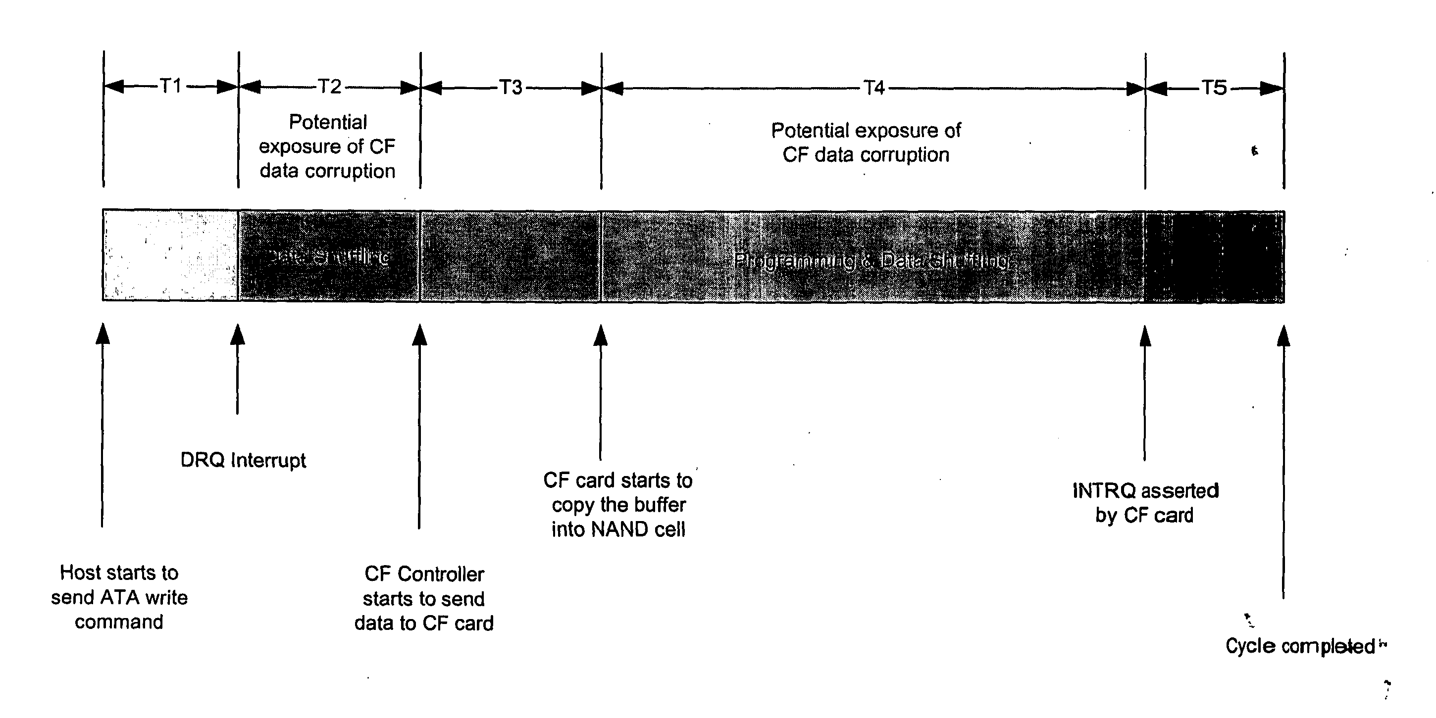
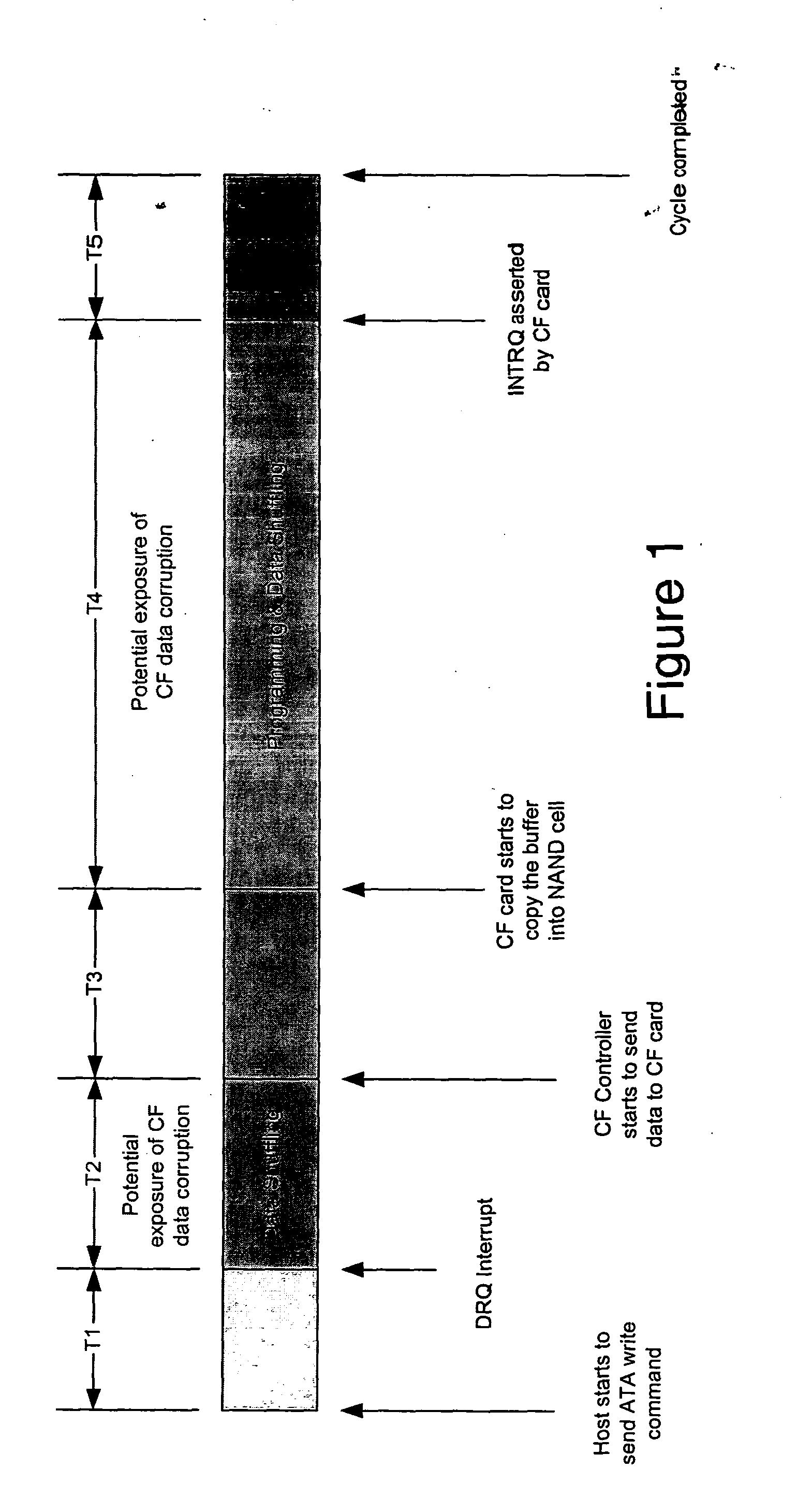
[0022]FIG. 1 illustrates one particular flash memory access cycle as a function of time. At the start of time segment T1 the CPU is sending an ATA write command; at the end of segment T1 the flash memory card asserts an interrupt to cause the DRQ bit to be set at the flash memory controller.

[0023] At the start of time segment T2, the DRQ bit is set at the flash memory controller; and, at the end of segment T2 the CPU responds to the interrupt.

[0024] At the start of time segment T3, the CPU writes data to the flash memory card buffer via the flash memory controller; at the end of segment T3, the flash memory card begins writing to the NAND flash memory device within the flash memory card.

[0025] At the start of time segment T4, the flash memory card has begun writing to the NAND flash memory device; at the end of segment T4, the flash memory card has completed the write and it asserts an interrupt to signal the completion of the write operation.

[0026] At the start of time segment ...


PUM


Abstract

The loss of data and / or the corruption of data that may occur in flash memory when a reset signal is received during a memory write cycle is prevented by delaying reset signals sent to the flash memory for a time period sufficient for a write cycle to be completed. The loss of data and / or the corruption of data that may occur in flash memory when the power supply is interrupted during a write cycle is prevented by providing a DC-to-DC converter with one or more large capacitors in parallel with its input as the power supply to the flash memory. If the system power supply fails or is interrupted, the discharge of the capacitor(s) delays the voltage decay at the input of the DC-to-DC converter such that the output of the DC-to-DC converter remains within tolerance for a time sufficient for the flash memory to complete a write cycle.

Description

BACKGROUND [0001] 1. Field of the Invention [0002] This invention relates to logic circuits having non-volatile memory. More specifically, it relates to reset signals sent to memory controllers for NAND-type flash memory and power supplies for NAND-type flash memory. [0003] 2. Description of the Related Art [0004] Flash is one type of non-volatile memory. EPROM (Erasable Programmable Read Only Memory) can be programmed and erased enabling them to be re-used. Erasure is accomplished using an UV (Ultra Violet) light source that shines through a quartz erasing window in the EPROM package. [0005] There also are OTP (One Time Programmable) EPROMs, sometimes called OTPROMs (One Time Programmable Read Only Memory), that are identical to an erasable EPROM but lack an erasing window to reduce costs. To reduce their cost these EPROMs come in a windowless plastic carrier, which is cheaper than the costly ceramic package required for the erasing window. They can be programmed one time only. [00...

Claims


Application Information

Patent Timeline
Patent Type & Authority Applications(United States)
IPC IPC(8): G11C16/30H03K19/003
CPCG11C16/30
Inventor LEE, MICHAEL K. T.DOAN, CHANH VAN
Owner AVAGO TECH INT SALES PTE LTD
Learn More