Structures and methods to enhance field emission in field emitter devices

a field emitter and electron emission technology, applied in the manufacture of electrode systems, cold cathode manufacturing, electric discharge tubes/lamps, etc., can solve the problems of difficulty in getting the field emitter to emit electrons, video images on these displays tend to take on undesired viewing characteristics, etc., to improve the releasing of electrons, inhibit degradation, and limit outgassing

Inactive Publication Date: 2005-02-03
MICRON TECH INC
View PDF24 Cites 5 Cited by
  • Summary
  • Abstract
  • Description
  • Claims
  • Application Information

AI Technical Summary

Benefits of technology

[0007] In particular, an illustrative embodiment of the present invention includes a field emitter display device. This device comprises at least one emitter having an implantation that releases electrons at a predetermined energy level. The implantation enhances the releasing of electrons. The implantation also acts to limit outgassing so as to inhibit the degradation of the at least one emitter. In one embodiment, this implantation is embedded in the surface of the emitter.

Problems solved by technology

Although field emitter displays promise to provide better color and image resolution, one of their problems is that it is difficult to get the field emitter to emit electrons so as to strike the phosphor target to generate the display.
Another problem is that video images on these displays tend to take on undesired viewing characteristics over a relative short period of time.
These undesired characteristics might be caused by degradation of the field emitter display due to certain conditions near the vicinity of the field emitter displays.
These issues raise questions about the commercial success of the displays in the marketplace.

Method used


Image

  • Structures and methods to enhance field emission in field emitter devices
  • Structures and methods to enhance field emission in field emitter devices
  • Structures and methods to enhance field emission in field emitter devices

Examples


Embodiment Construction

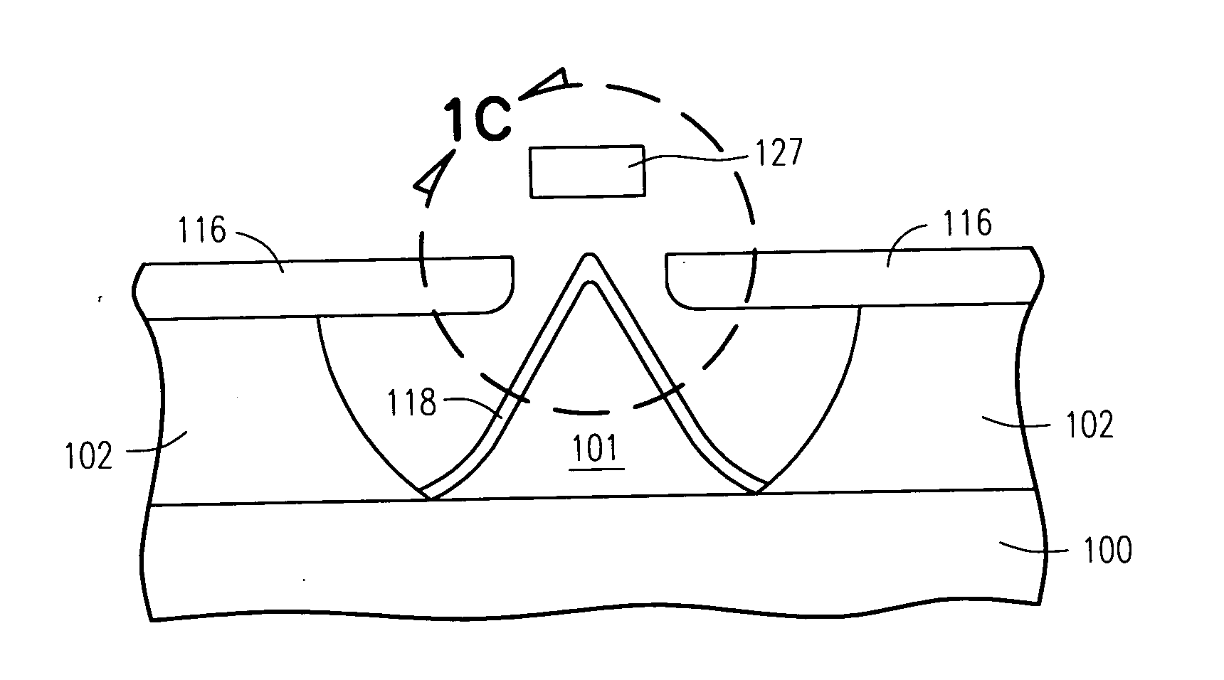
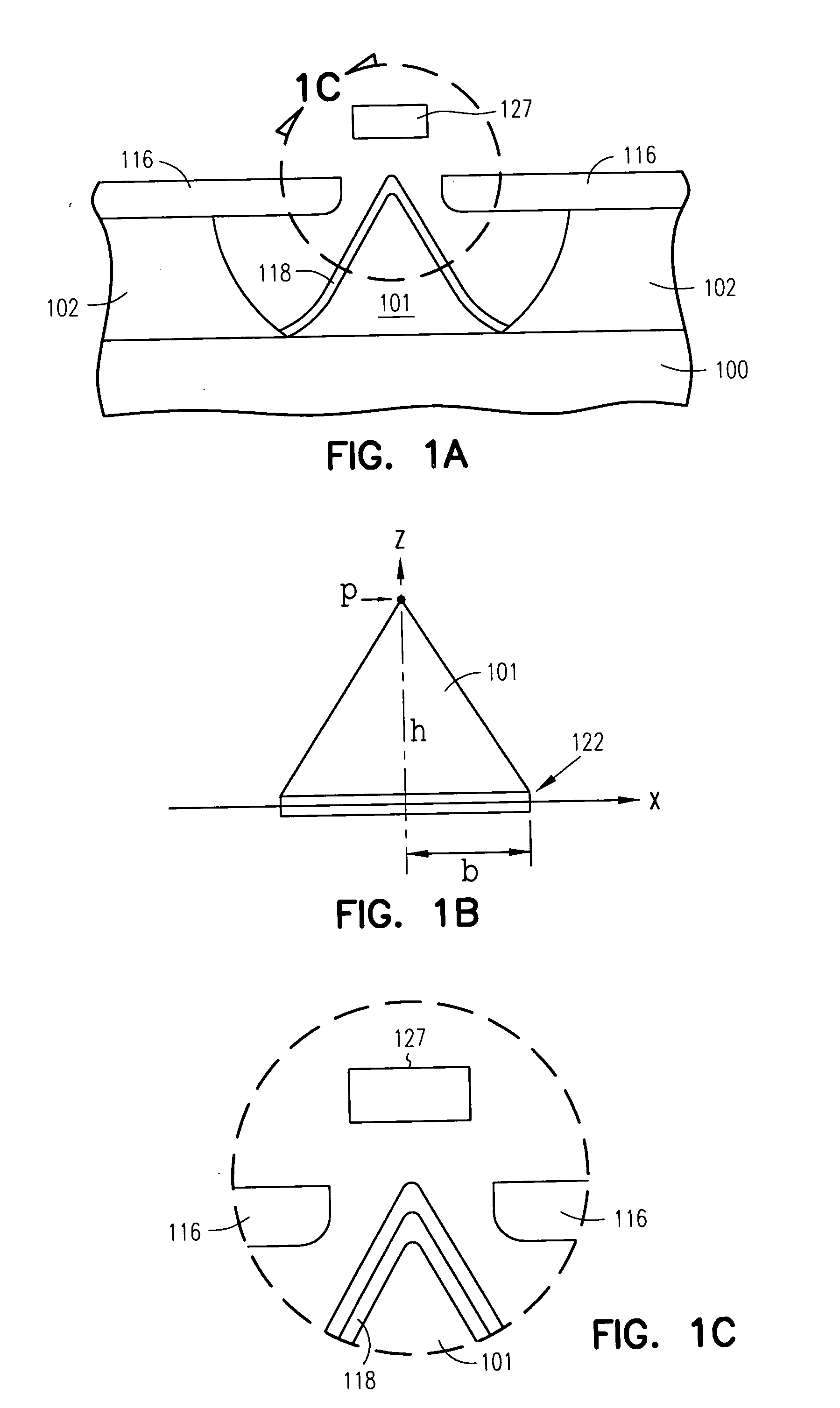
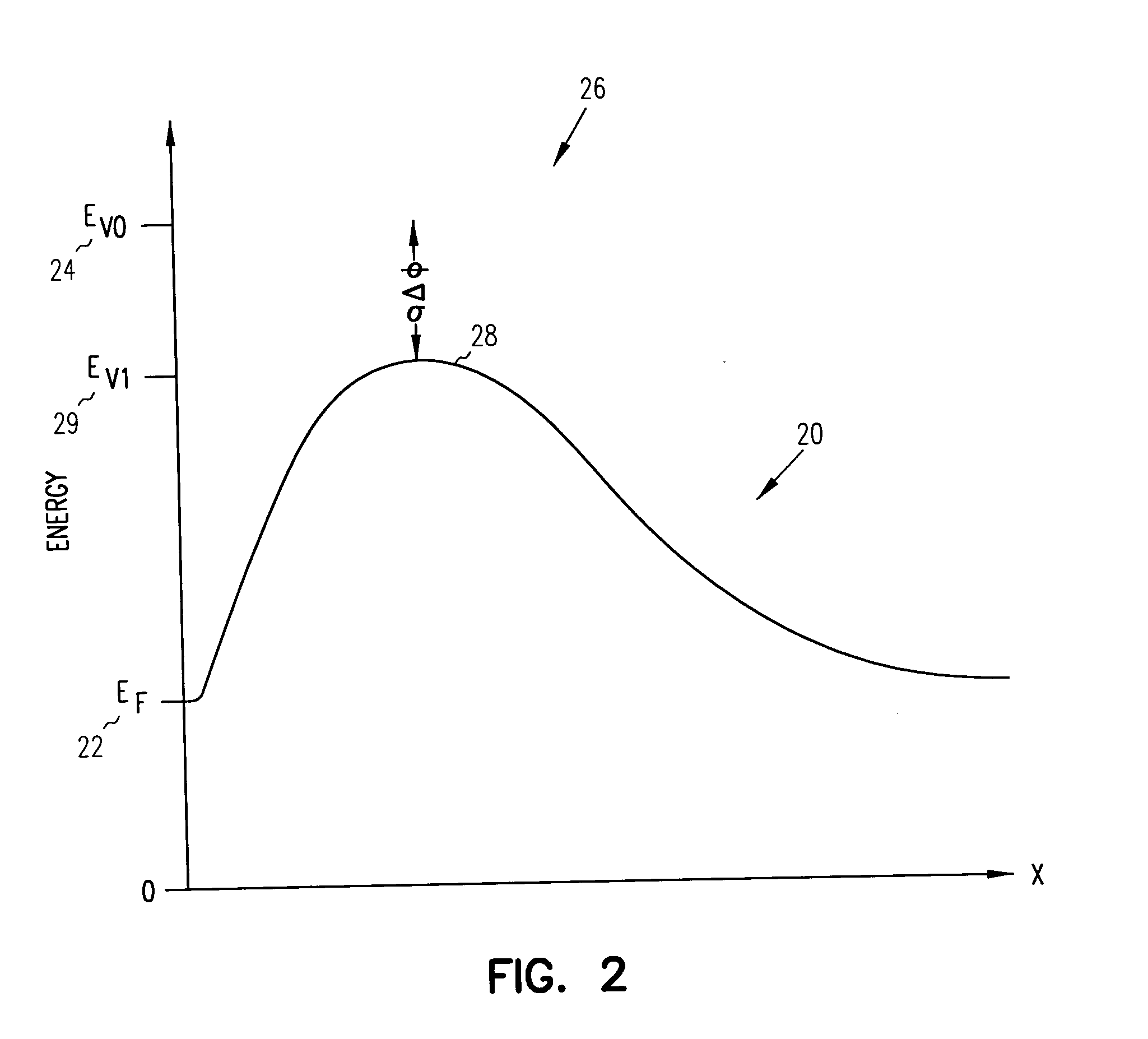
[0017] In the following detailed description of the invention, reference is made to the accompanying drawings which form a part hereof, and in which is shown, by way of illustration, specific embodiments in which the invention may be practiced. In the drawings, like numerals describe substantially similar components throughout the several views. These embodiments are described in sufficient detail to enable those skilled in the art to practice the invention. Other embodiments may be utilized and structural, logical, and electrical changes may be made without departing from the scope of the present invention.

[0018] The terms wafer and substrate used in the following description include any structure having an exposed surface with which to form the integrated circuit (IC) structure of the invention. The term substrate is understood to include semiconductor wafers. The term substrate is also used to refer to semiconductor structures during processing, and may include other layers that...


PUM


Abstract

Structures and methods to ease electron emission and limit outgassing so as to inhibit degradation to the electron beam of a field emitter device are described. In one method to ease such electron emission, a layer of low relative dielectric constant material is formed under the surface of the field emitter tip. Another method is to coat the field emitter tip with a low relative dielectric constant substance or compound to form a layer and then cover that layer with a thin layer of the material of the field emitter tip.

Description

[0001] This application is a Divisional of U.S. application Ser. No. 09 / 387,164, filed Aug. 31, 1999 which is incorporated herein by reference.FIELD OF THE INVENTION [0002] The present invention relates generally to semiconductor integrated circuits. More particularly, it pertains to structures and methods to enhance electron emission in a field emitter device. BACKGROUND OF THE INVENTION [0003] Recent years have seen an increased interest in field emitter displays. This is attributable to the fact that such displays can fulfill the goal of being consumer-affordable hang-on-the-wall flat panel television displays with diagonals in the range of 20 to 60 inches. Certain field emitter displays operate on the same physical principles as cathode ray tube (CRT) based displays. Excited electrons are guided to a phosphor target to create a display. The phosphor then emits photons in the visible spectrum. This method of operation for field emitter displays relies on an array of field emitter...

Claims


Application Information

Patent Timeline
Patent Type & Authority Applications(United States)
IPC IPC(8): H01J1/304H01J9/02
CPCH01J1/3044H01J2201/30426H01J9/025
Inventor HU, YONGJUN
Owner MICRON TECH INC
Why Eureka
Try Eureka