Solid state image pickup device and method of fabricating the same

Inactive Publication Date: 2005-02-17
SONY SEMICON SOLUTIONS CORP
View PDF1 Cites 1 Cited by
  • Summary
  • Abstract
  • Description
  • Claims
  • Application Information

AI Technical Summary

Benefits of technology

[0007] In view of the foregoing, it is an object of the present invention to provide a solid state image pickup device and a method of fabricating the same by which it is possible to suppress a rise in contact resistance attendant on a heat treatment in a later step, in a structure wherein there is provided a contact between various wirings and a light shielding film using a high melting point metal and a Si substrate and Si-containing electrodes, wirings, or the like conductive patterns, to improve propagation characteristics of various signals, and to contribute to provision of an image pickup device with a higher speed, a larger size, a higher image quality, etc.
[0011] According to another aspect of the present invention, there is provided a method of fabricating a solid state image pickup device in which, first, an insulating film covering a conductive pattern (namely, the above-mentioned transfer electrode, the buffer wiring, or the like) formed above a substrate is provided with a contact window reaching the substrate or the conductive pattern. Next, the bottom surface of the contact window is covered with a thin film composed of at least one of silicon oxide and silicon nitride. Subsequently, a metallic pattern (namely, the above-mentioned shunt wiring or the light shielding film) is formed above the upper side of the insulating film. At a bottom portion of the contact window, the metallic pattern is so shaped as to be connected to the substrate or the conductive pattern via the thin film. Thereafter, a heat treatment is conducted to cause the silicon oxide or silicon nitride constituting the thin film and the metal constituting the metallic pattern to react with each other at the bottom surface portion of the contact window, thereby contriving a lowering of the connection resistance between the substrate or the conductive pattern and the metallic pattern.
[0013] As has been mentioned above, according to the solid state image pickup device of the present invention, the contact portion between the metallic pattern such as a shunt wiring, a light shielding film, etc. and the conductive pattern composed of silicon such as the substrate, the transfer electrode, etc. contains silicon metal oxide or silicon metal nitride. As a result, the connection resistance at the connection portion can be suppressed, as compared with the case where a layer forming metallic oxide or metallic nitride is sandwiched between the metallic pattern and the conductive pattern. Therefore, it is possible to connect the wiring and the electrode with a low resistance, to improve propagation characteristics of various signals, to transfer a signal such as a clock pulse at a high speed without causing deterioration of the waveform, and to contrive to provision of an image pickup device with a higher speed, a larger size, a higher image quality, etc.
[0014] Besides, according to the method of fabricating a solid state image pickup device of the present invention, a heat treatment is conducted under the condition where a thin film composed of silicon oxide or silicon nitride is laminated at the connection portion between the metallic pattern such as a shunt wiring, a light shielding film, etc. and the conductive pattern such as a substrate, a transfer electrode, etc., whereby it is possible to contrive a further lowering of resistance at the connection portion while preventing the volume expansion at the connection portion. Accordingly, it is possible to connect the wiring and the electrode with a low resistance, to improve propagation characteristics of various signals, to transfer a signal such as a clock pulse at a high speed without causing deterioration of the waveform, and to contribute to provision of an image pickup device with a higher speed, a larger size, a higher image quality, etc.

Problems solved by technology

However, since the resistance of the poly-Si film is high, in the case where clock rate is high or where transmission distance is long, propagation of a signal transmitted through the transfer-accumulation electrode would be delayed.
Particularly, it is difficult to obtain an image pickup device with a higher driving speed and a larger area.
However, in the conventional shunt structure mentioned above, in the case where a high melting point metal is used as the material of the shunt wiring, there is the problem that a heat treatment conducted after the formation of the insulating film above the light shielding film 26 would raise the contact resistance between the shunt wiring 22 and the transfer-accumulation electrodes 14, 16 or the buffer wiring 18.
Therefore, there has been a limit to the suppression of the contact resistance between the high melting point metal and silicon.

Method used


Image

  • Solid state image pickup device and method of fabricating the same
  • Solid state image pickup device and method of fabricating the same
  • Solid state image pickup device and method of fabricating the same

Examples


Embodiment Construction

[0023] Now, an embodiment of the present invention will be described in detail below, referring to the drawings. The following embodiment is a specific example of application of the present invention to a CCD image sensor, and technically preferable various limitations are added thereto, but the scope of the present invention is not limited to the embodiments, unless a description that the present invention is to be limited is particularly given in the following description.

[0024]

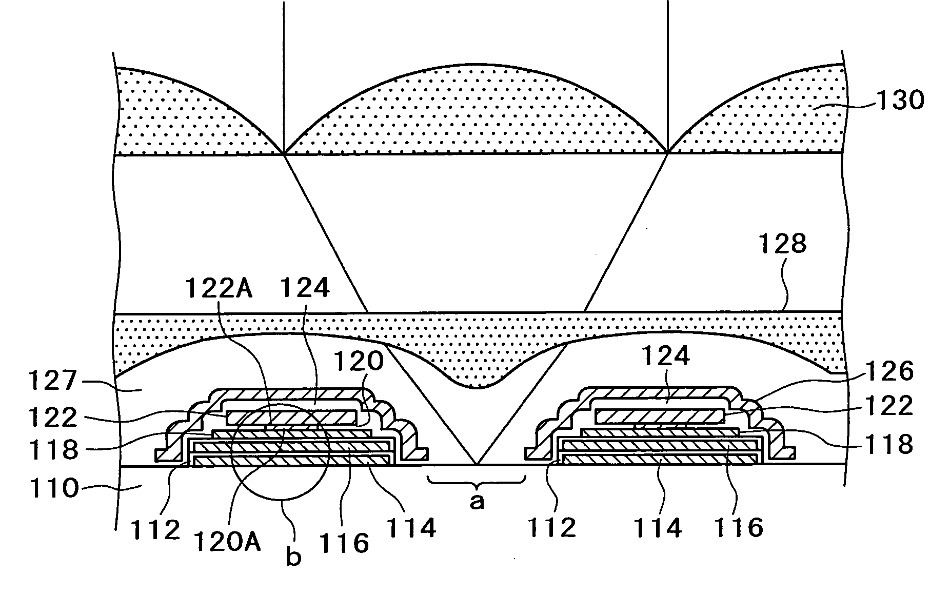
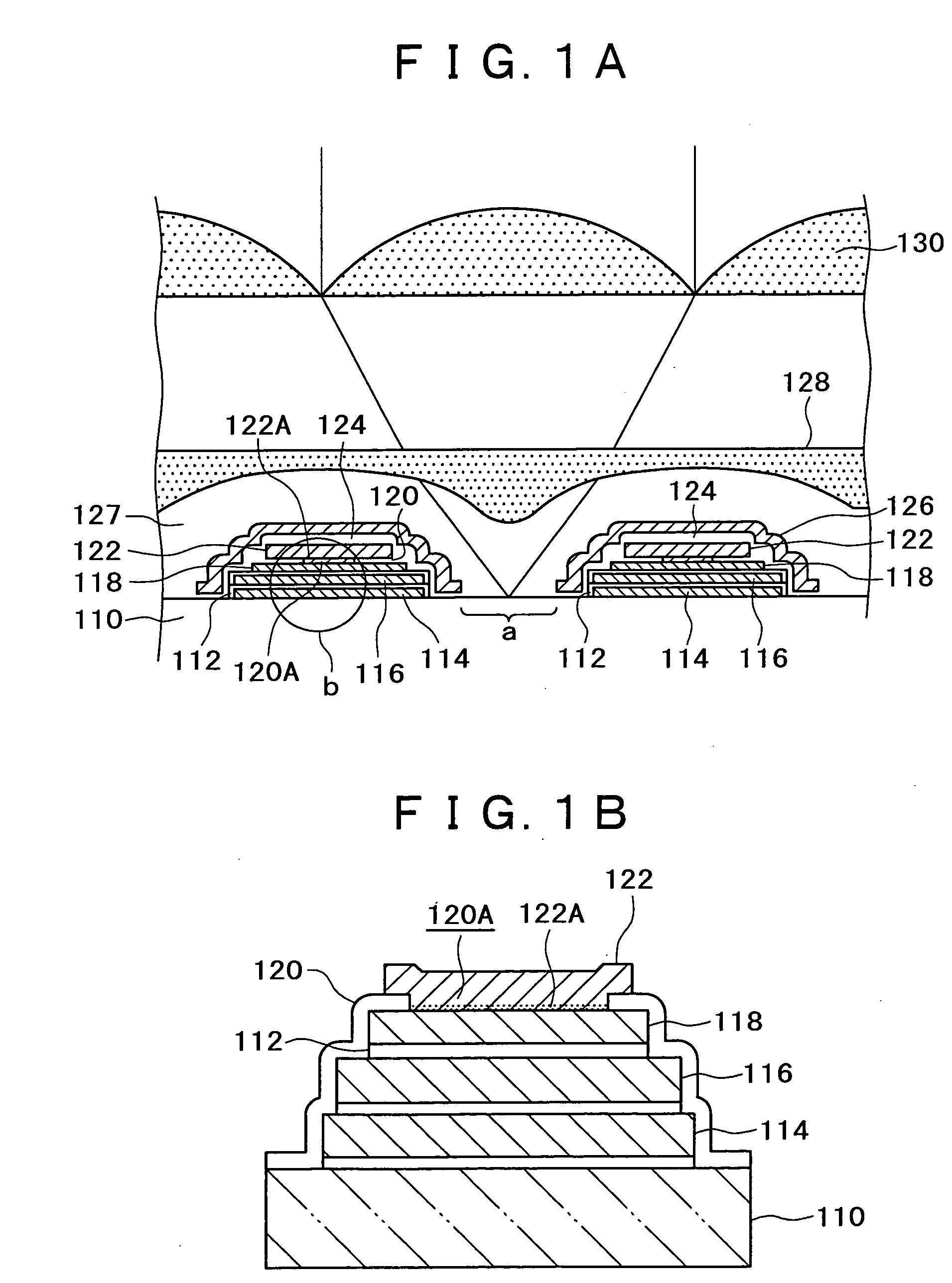
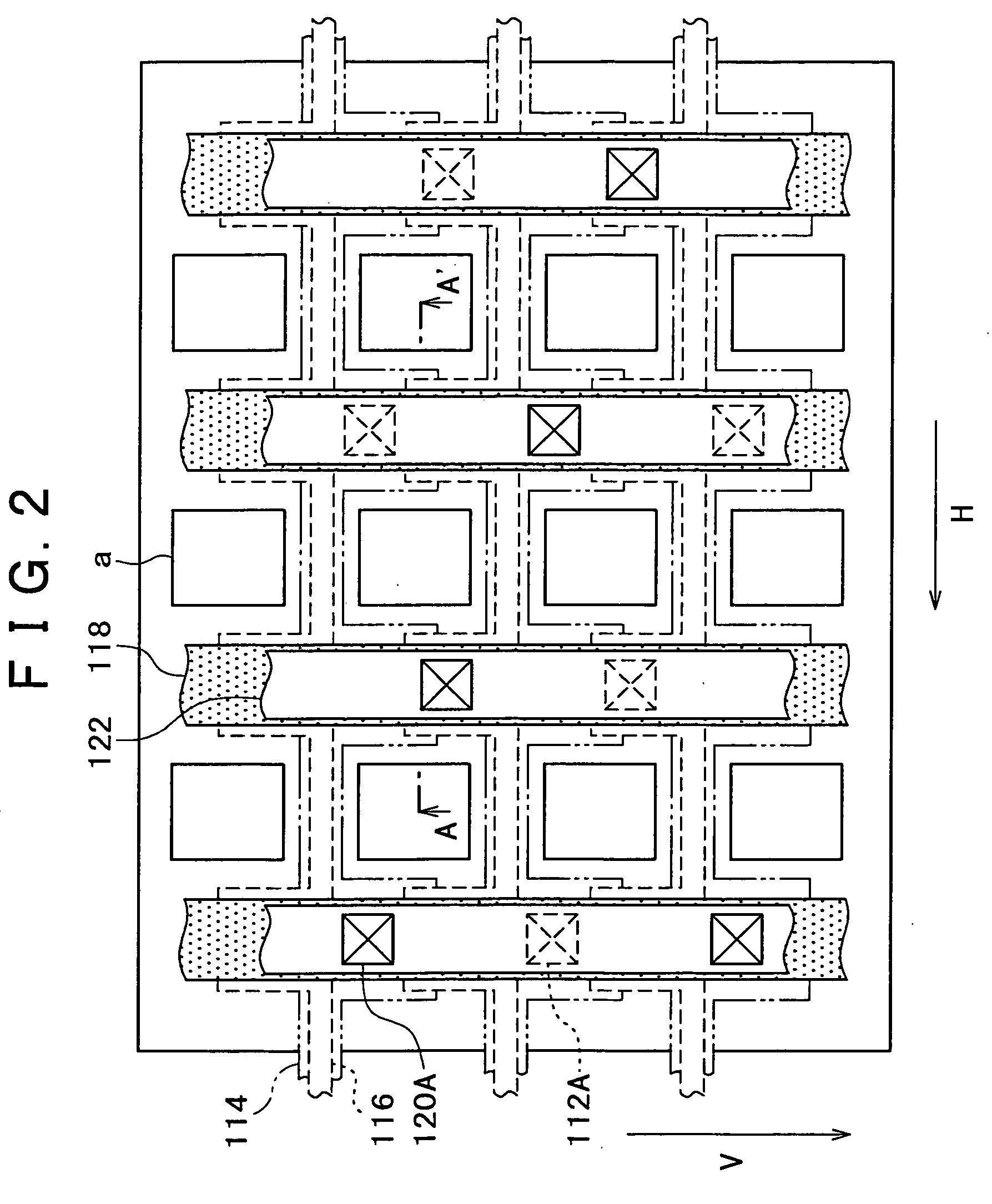
[0025]FIGS. 1A, 1B, and 2 are schematic views of a portion at and around a pixel of a CCD image sensor using a shunt structure according to an embodiment of the present invention, illustrating an example where a buffer wiring is provided between a transfer-accumulation electrode and a shunt wiring. Of these figures, FIG. 1A is an A-A′ sectional view (a sectional view taken along a horizontal transfer direction H orthogonal to a vertical transfer direction V) in a general plan view of an image pickup region...


PUM


Abstract

Disclosed is a solid state image pickup device including a Si substrate, a conductive pattern such as transfer-accumulation electrodes and a buffer wiring formed above the Si substrate, an insulating film provided above the Si substrate in the state of covering the conductive pattern, and a shunt wiring composed of a metallic pattern formed above the insulating film in the state of being connected to the buffer wiring via a contact window formed in the insulating film. The portion of the shunt wiring in the vicinity of the bottom surface of the contact window contains at least one of silicon metal oxide or silicon metal nitride. The solid state image pickup device and a method of fabricating the same make it possible to suppress a rise in the contact resistance attendant on a heat treatment in a later step, in a structure in which various wirings and a light shielding film using a metallic material and a conductive pattern such as a Si substrate and a Si-containing electrode or wiring are brought into contact with each other, to improve propagation characteristics of various signals, and to contribute to provision of an image pickup device with a higher speed, a larger size, a higher image quality, etc.

Description

BACKGROUND OF THE INVENTION [0001] Hitherto, in a transfer portion of a CCD image sensor, for example, a poly-Si (polycrystalline silicon) film is used for constituting a transfer-accumulation electrode disposed on a buried CCD register. However, since the resistance of the poly-Si film is high, in the case where clock rate is high or where transmission distance is long, propagation of a signal transmitted through the transfer-accumulation electrode would be delayed. Particularly, it is difficult to obtain an image pickup device with a higher driving speed and a larger area. In order to solve such a problem, a shunt structure has been used in which a shunt wiring is disposed above the upper side of the transfer-accumulation electrode and a clock signal is supplied to the transfer-accumulation electrode through the shunt wiring, to thereby obviate the clock signal propagation delay and to achieve an image pickup device with a higher speed and a larger area. As the material of the shu...

Claims


Application Information

Patent Timeline
IPC IPC(8): H01L21/3205H01L21/768H01L23/52H01L27/12H01L27/14H01L27/146H01L27/148
CPCH01L27/12H01L27/14623H01L27/14812H01L27/14627H01L27/14625H01L27/148
Inventor MARUYAMA, YASUSHI
Owner SONY SEMICON SOLUTIONS CORP
Why Eureka
Try Eureka