
Photoelectric converter and a method of driving the same

Active Publication Date: 2005-02-17
ABLIC INC
View PDF1 Cites 7 Cited by
  • Summary
  • Abstract
  • Description
  • Claims
  • Application Information

AI Technical Summary

Benefits of technology

[0017] Consequently, it becomes possible to supply an image sensor IC having a simple configuration and a small fluctuation in dark outputs. Moreover, it is possible to provide a highly accurate close contact type image sensor in which a plurality of image sensor ICs are linearly mounted.

Problems solved by technology

This leads to such a problem that reset noises put on the reference signal and the optical signal are different from each other.
That is, because the reset noises of the different timings are compared with each other, there arises a problem in that the random noises are large.

Method used


Image

  • Photoelectric converter and a method of driving the same
  • Photoelectric converter and a method of driving the same
  • Photoelectric converter and a method of driving the same

Examples


first embodiment

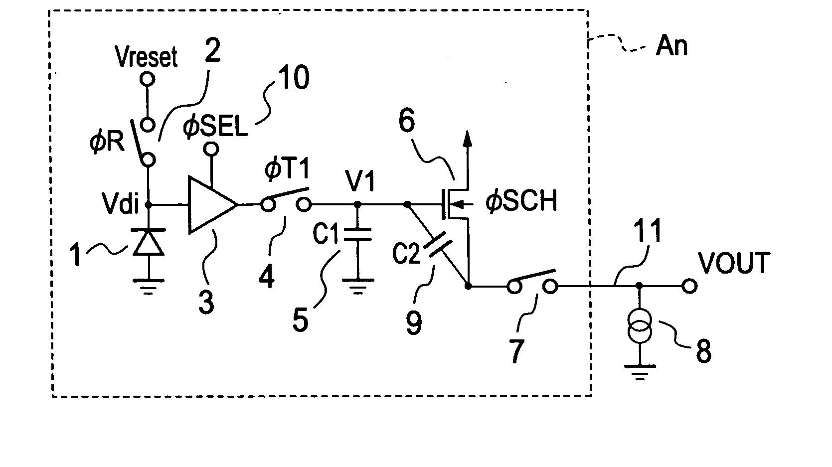
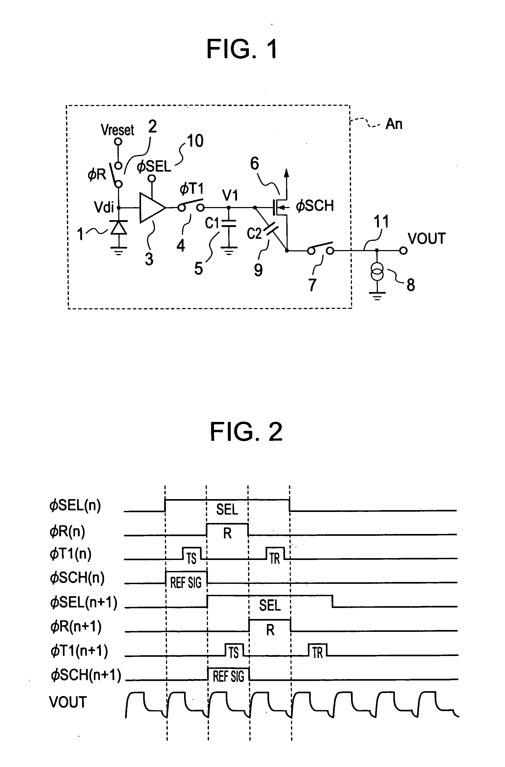
[0036]FIG. 1 is a schematic circuit diagram of a sequential type photoelectric converter according to a first embodiment of the present invention. The sequential type photoelectric converter means a photoelectric converter for carrying out reset of electric charges and storage of photocharges in an output of each photodiode of an image sensor in parallel with each other while shifting a timing.

[0037] A photoelectric conversion block An shows a photoelectric conversion block of an n-th bit. The number of photoelectric conversion blocks is identical to the number of pixels, and the photoelectric conversion blocks are connected to a common signal line 11 through the respective channel selection switches 7. A configuration of a whole photoelectric converter is shown in FIG. 7.

[0038] A circuit of this embodiment includes: a photodiode 1 serving as a photoelectric conversion unit; a reset switch 2 serving as a reset unit; an amplification unit 3; a transfer switch 4 serving as an electr...

second embodiment

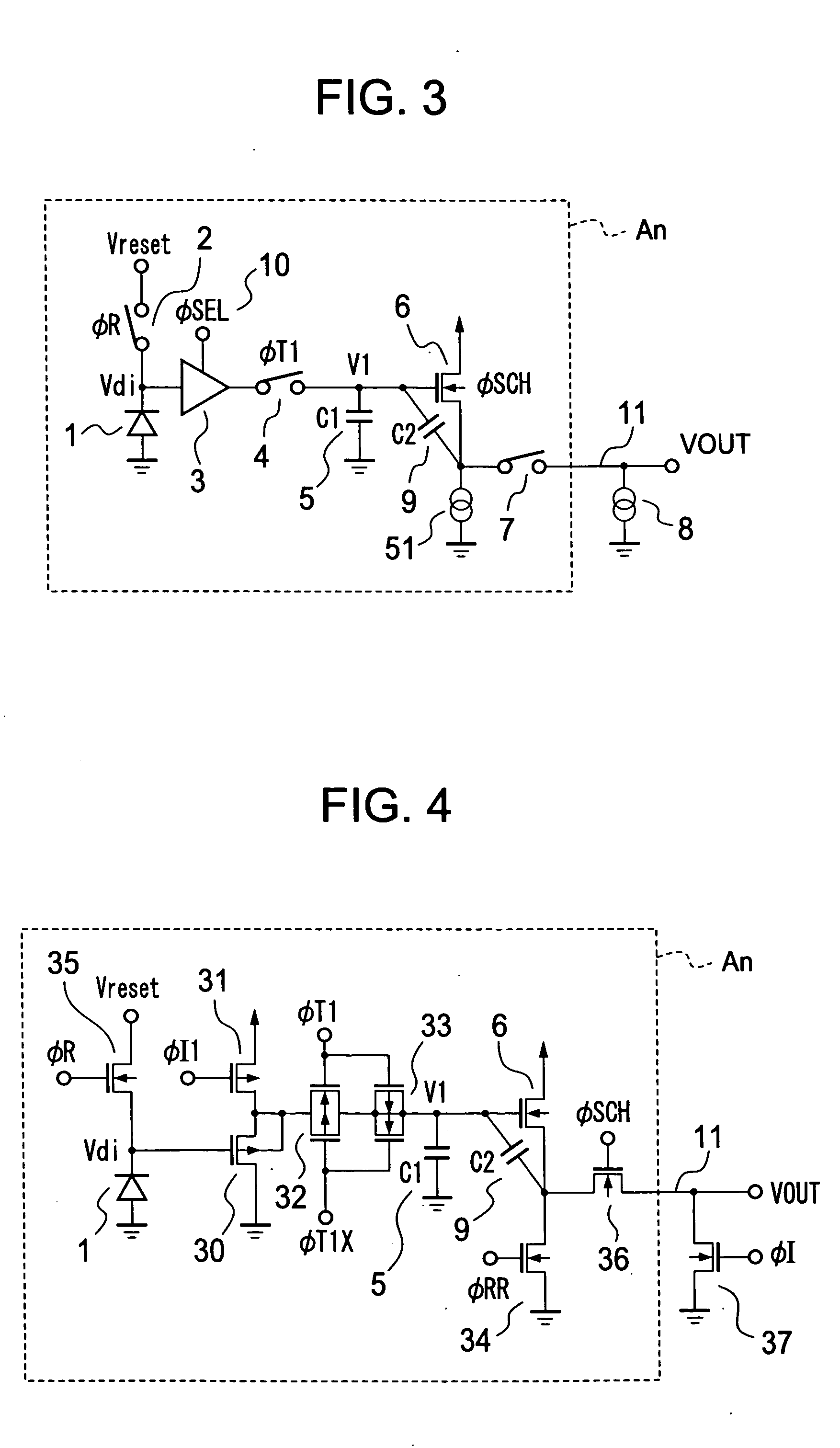
[0047]FIG. 3 is a schematic circuit diagram of a sequential type photoelectric converter according to a second embodiment of the present invention. A point of difference in configuration from FIG. 1 is that a second current source 51 is connected to a source of the MOS transistor 6. The second current source 51 is designed so that it is turned ON and OFF in accordance with an enable signal ΦRR, and while the second current source 51 is held in an ON state, a current which is substantially the same as that of the first current source 8 is caused to flow through the second current source 51.

[0048]FIG. 5 is a timing chart corresponding to the schematic circuit diagram of the sequential type photoelectric converter according to the second embodiment of the present invention.

[0049] At the time when the reset switch 2 is turned ON in accordance with ΦR(n), a voltage appearing at an output terminal Vdi of the photodiode 1 is fixed to a reference voltage Vreset. On the other hand, at the ...

third embodiment

[0061]FIG. 8 is a schematic circuit diagram of a batch type photoelectric converter according to a third embodiment of the present invention. The batch type photoelectric converter means a photoelectric converter for carrying out reset of electric charges and storage of photocharges in the output of each photodiode of the image sensor in parallel with each other and at the same timing. A photoelectric conversion block An shows a photoelectric conversion block of an n-th bit. The number of photoelectric conversion blocks is identical to the number of pixels, and the photoelectric conversion blocks are connected to the common signal line 11 through the respective channel selection switches 7. A diagram of a configuration of the whole photoelectric converter is shown in FIG. 7.

[0062] The circuit of this embodiment includes: the photodiode 1 serving as a photoelectric conversion unit; transfer switches 18, 19 and 20 each serving as an electric charge transfer unit; a reset switch 2 ser...


PUM


Abstract

The invention provides a photoelectric converter capable of reducing a random noise. The photoelectric converter includes: a photoelectric conversion unit having an output terminal connected to input terminals of a reset unit and an amplification unit; a hold unit for holding a reference signal generated through resetting of the output terminal of the photoelectric conversion unit; and a signal read unit for reading out to a common signal line the reference signal and an optical signal obtained after storage of electric charges generated on the basis of light made incident to a photoelectric conversion area of the photoelectric conversion unit.

Description

BACKGROUND OF THE INVENTION [0001] 1. Field of the Invention [0002] The present invention relates to a photoelectric converter that receives a light reflected from an original to which the light is irradiated, and converts the light into an electric signal, and more specifically to a linear image sensor suitable for an image reading device such as a facsimile or an image scanner. [0003] 2. Description of the Related Art [0004]FIG. 16 shows a circuit diagram of an image sensor IC used in a conventional image reading device, and FIG. 17 shows a timing chart. (For example see JP 11-239245 A (pages 2 through 5, FIG. 1)). [0005] An N-type region of a photodiode 101 is connected to a positive supply voltage terminal VDD, and a P-type region is connected to a drain of a reset switch 102 and a gate of a source follower amplifier 103. A source of the reset switch 102 is supplied with a reference voltage VREF1. A source of the output terminal of the source follower amplifier 103 is connected ...

Claims


Application Information

Patent Timeline
IPC IPC(8): H01L31/00H01L27/146H04N1/028H04N5/335H04N5/357H04N5/369
CPCH04N3/1568H04N5/3692H04N5/363H04N25/616H04N25/65H04N25/701
Inventor MACHIDA, SATOSHIKAWAHARA, YUKITO
Owner ABLIC INC
Learn More