Semiconductor package having light sensitive chips

a technology of semiconductor and light-emitting chips, which is applied in the direction of semiconductor devices, semiconductor/solid-state device details, electrical apparatus, etc., can solve the problems of large area consumed by the chip package manufactured in accordance with the prior art methods described above, large area consumed by the printed circuit board or the electronic component that might otherwise be required, and particular prior art embodiments are also relatively complex and expensive. , to achieve the effect of less footprint, less transparency or translucency, and easy flex

Inactive Publication Date: 2005-02-17
TESSERA INC
View PDF28 Cites 28 Cited by
  • Summary
  • Abstract
  • Description
  • Claims
  • Application Information

AI Technical Summary

Benefits of technology

[0013] In certain preferred embodiments of the present invention the encapsulant has different levels of transparency or translucency. For example, in one particular preferred embodiment the encapsulant overlying the optical area of the optoelectronic element is more transparent than the encapsulant overlying the periphery thereof. The encapsulant may also include a compliant material whereby the gradient of compliancy varies throughout the package. In one particular embodiment the encapsulant adjacent the chip contacts is more compliant than the encapsulant adjacent the at least one conductive pads. This particular feature enables the conductive wires or leads adjacent the contacts to readily flex and move as the light sensitive chip or light emitting chip expands and contracts during operation. In still other preferred embodiments the encapsulant includes a color tinted portion for changing the color of the emitted light as perceived by an observer. For example, the light emitted from the optoelectronic element may be red and the encapsulant may have a blue tint so that the emitted light as perceived by an observer is purple.
[0014] Certain preferred embodiments of the present invention provide near “chip size” microelectronic packages having light sensitive or light emitting chips whereby the overall size of the package is not much larger than the size of the chip itself. Thus, the final packages have a smaller footprint and will take up less space on a circuit board or within an electronic component which enables the overall size of the final electronic product to be reduced. This is a dramatic advance over prior art packages which teach using bulky substrates which generally dwarf the size of the chip so as to create packages which are much larger than the chip being packaged, thereby wasting a significant amount of space within an electronic device. The present invention also provides methods for mass producing reliable and economical chip packages.

Problems solved by technology

The chip packages manufactured in accordance with the prior art methods described above typically consume greater areas on a printed circuit board or within an electronic component than might otherwise be required.
In addition, these particular prior art embodiments are also relatively complex and expensive.

Method used


Image

  • Semiconductor package having light sensitive chips
  • Semiconductor package having light sensitive chips
  • Semiconductor package having light sensitive chips

Examples


Embodiment Construction

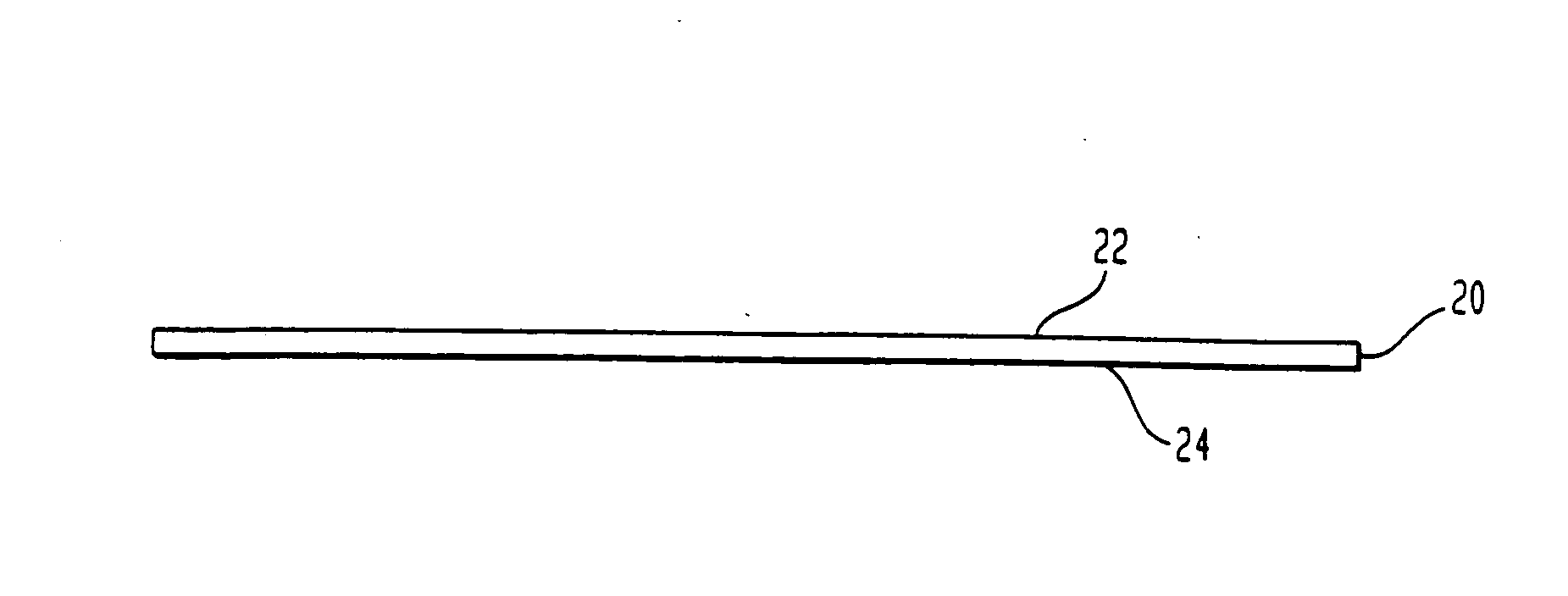
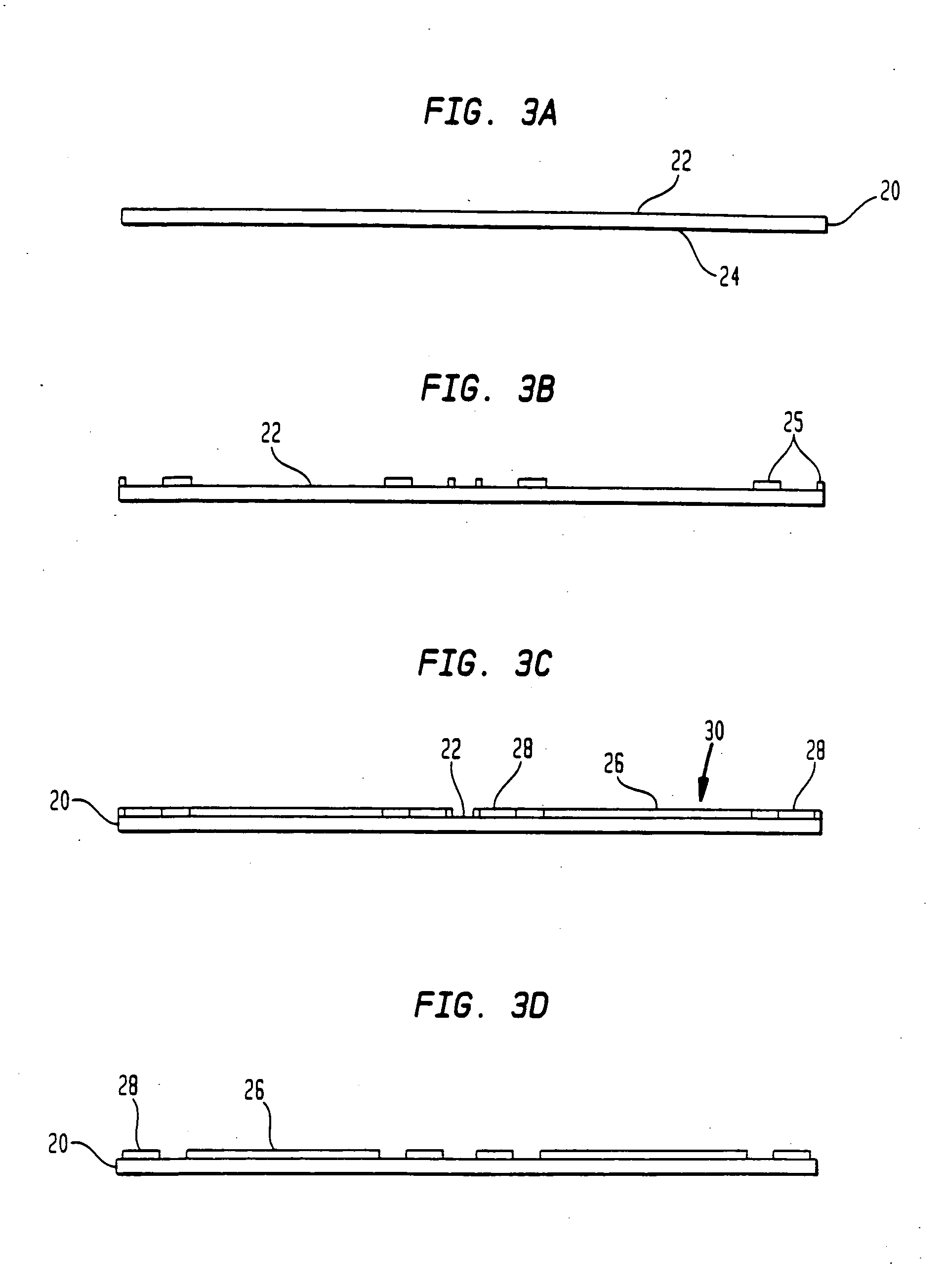
[0031]FIGS. 3A through 3I show a method for making a package having a semiconductor chip such as a light sensitive chip, according to one preferred embodiment of the present invention. The method described is somewhat similar to the process disclosed in U.S. patent application Ser. No. 08 / 634,464, filed on Apr. 18, 1996, the disclosure of which is hereby incorporated by reference herein. As shown in FIG. 3A, a sacrificial layer 20 is provided having a first surface 22 and a second surface 24. The sacrificial layer 20 may include a conductive metallic material, a polymer material or a combination of both. Specific examples of preferred sacrificial layer materials include aluminum, copper, steel, iron, bronze, brass, polyimide, polyetherimide, flouropolymer and alloys and combinations thereof. In the particular embodiment shown in FIG. 3A, the sacrificial layer 20 includes a sheet of aluminum having an approximate substantially uniform thickness of about 100-200 microns; although, the...


PUM


Abstract

A microelectronic package includes a light sensitive microelectronic element having a front face including one or more contacts and a rear surface, and conductive leads having first ends connected to the one or more contacts and second ends connected to one or more conductive pads adjacent the light sensitive microelectronic element. The package also includes an at least partially transparent encapsulant covering the light sensitive microelectronic element, the conductive leads and the one or more conductive pads, whereby the one or more conductive pads are exposed on a surface of the encapsulant.

Description

CROSS REFERENCE TO RELATED APPLICATIONS [0001] The present application is a continuation of U.S. patent application Ser. No. 10 / 342,973, which is a continuation of U.S. patent application Ser. No. 09 / 025,558, which claims benefit of U.S. Provisional Application 60 / 038,214, filed Feb. 18, 1997, and is related to U.S. patent application Ser. No. 08 / 634,464 filed Apr. 18, 1996, the disclosures of which are hereby incorporated by reference herein.BACKGROUND OF THE INVENTION [0002] The present invention generally relates to microelectronic assemblies, and more specifically it relates to semiconductor chip packages having light sensitive or light emitting chips. [0003] The semiconductor chip packaging industry is a highly competitive business in which the packaging companies are waging an on-going battle to improve the reliability and cost of packaged chips. Moreover, the electronics industry continues to demand that chip packages take up less space within electronic components. As such, ...

Claims


Application Information

Patent Timeline
Patent Type & Authority Applications(United States)
IPC IPC(8): H01L21/48H01L21/56H01L21/68H01L31/0203
CPCH01L2924/12041H01L21/4832H01L21/56H01L21/561H01L21/568H01L24/32H01L24/97H01L31/0203H01L2221/68377H01L2224/32245H01L2224/32257H01L2224/48091H01L2224/48228H01L2224/4824H01L2224/48247H01L2224/48465H01L2224/48472H01L2224/48475H01L2224/73265H01L2224/85001H01L2224/85051H01L2224/92H01L2224/92247H01L2224/97H01L2924/01002H01L2924/01009H01L2924/01013H01L2924/01029H01L2924/01047H01L2924/0105H01L2924/01077H01L2924/01079H01L2924/01082H01L2924/14H01L2924/1815H01L2924/01005H01L2924/01033H01L2924/18165H01L2224/48227H01L2924/00014H01L2224/85H01L2224/83H01L2924/00H01L2924/00012H01L24/73
Inventor FJELSTAD, JOSEPH
Owner TESSERA INC
Why Eureka
Try Eureka