Circuit and method to protect EEPROM data during ESD events

Inactive Publication Date: 2005-02-17
EL SHERIF ALAA Y +1
View PDF12 Cites 7 Cited by
  • Summary
  • Abstract
  • Description
  • Claims
  • Application Information

AI Technical Summary

Benefits of technology

[0004] The present invention achieves technical advantages as a circuit and method for greatly reducing or eliminating the risk of ESD induced reprogramming or erasure while retaining the ability to program the device in package. ESD is a nearly instantaneous event. The present invention overcomes the difficulty posed by this fact with a combination of circuits that delay the propagation of the high voltage spike and then clamp internal nodes under ESD conditions.
[0005] Other ESD protection methods require the EEPROM bits to be trimmed for optimum performance at the wafer level with a multi-probe test via an additional internal probe pad. Disadvantageously, some parameters can shift in the process of dicing each IC from the wafer, mounting it on a lead frame and encapsulating it in a plastic package. Thus, a circuit and method of EEPROM programming after packaging the device is desired. Accordingly, performance loss can be eliminated if the device is programmed after packaging and better yield levels can be achieved during the final test of packaged parts. The present invention advantageously retains the ability to program the device in package while greatly reducing or eliminating the risk of ESD induced reprogramming. Also, there is no need for an additional probe pad required by other solutions.

Problems solved by technology

Disadvantageously, some parameters can shift in the process of dicing each IC from the wafer, mounting it on a lead frame and encapsulating it in a plastic package.

Method used


Image

  • Circuit and method to protect EEPROM data during ESD events
  • Circuit and method to protect EEPROM data during ESD events
  • Circuit and method to protect EEPROM data during ESD events

Examples


Embodiment Construction

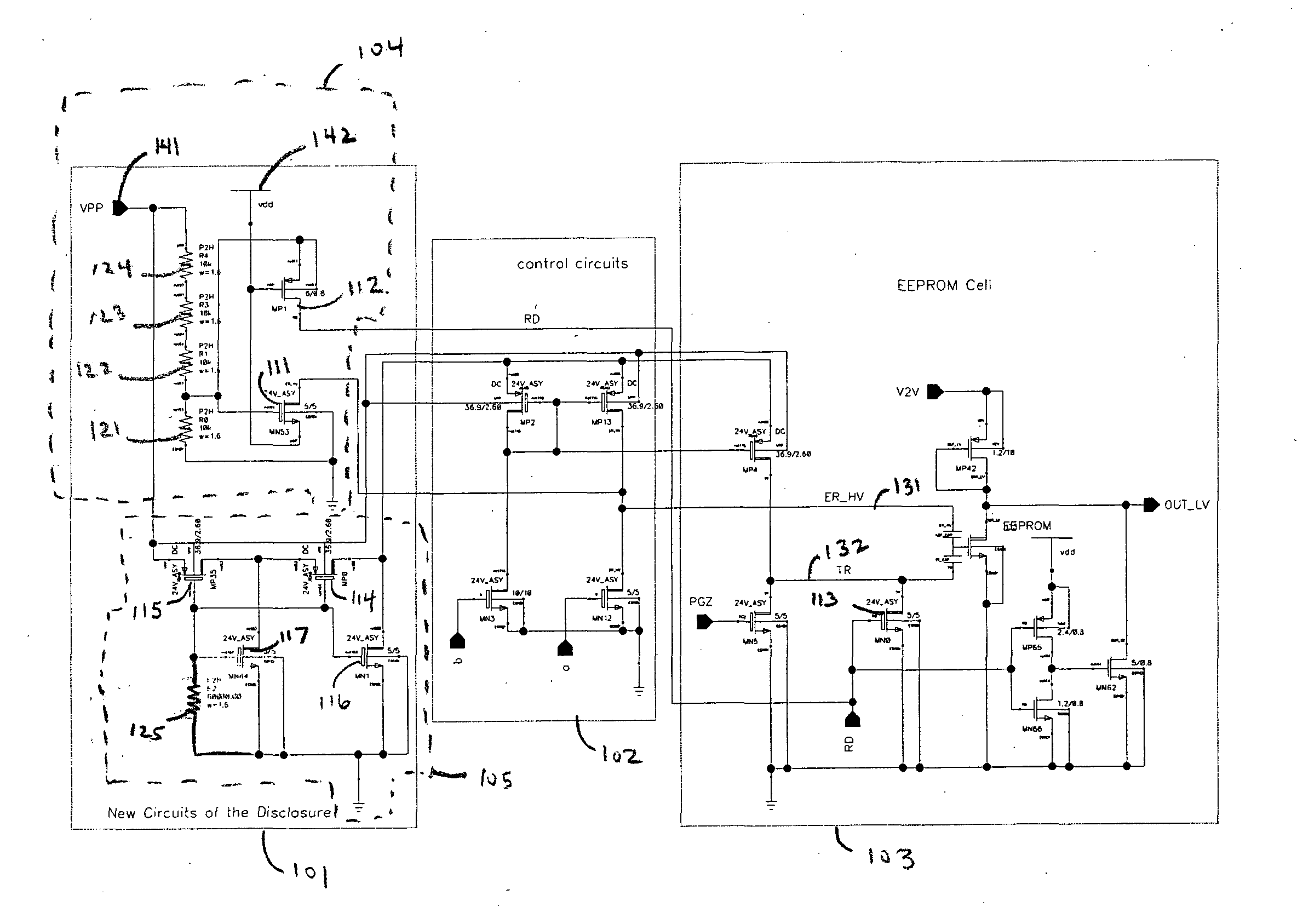
[0009] The numerous innovative teachings of the present invention will be described with particular reference to an exemplary embodiment. However, it should be understood that the exemplary embodiment is only one example of the many advantageous embodiments and innovative teachings herein. In general, statements made in the specification of the application do not necessarily delimit any of the various claimed inventions. Moreover, some statements may apply to some inventive features, but not to others. Detailed descriptions of known functions and constructions unnecessarily obscuring the subject matter of the present invention have been omitted for clarity.

[0010] A small number of EEPROM cells, typically less than one hundred bits, is used on servo motor controller ICs, including CMOS monolithic integrated circuits, as a cost effective means of fine tuning the performance of the silicon and reducing the effect of manufacturing variations. The bits are programmed by applying a signa...


PUM


Abstract

The present invention comprises a clamp circuit (104) comprised of a first transistor (111), a second transistor (112), a voltage divider circuit and a delay circuit (105) comprised of a fourth transistor (114), a fifth transistor (115), a sixth transistor (116) and a seventh transistor (117) and a fifth resistor (125), operable to keep the signals at the EEPROM input nodes (131) and (132) of a data cell, such as an EEPROM cell below a certain voltage threshold, preferable below 10 volts.

Description

FIELD OF THE INVENTION [0001] The present invention generally relates to circuits and method for minimizing the effects of electrostatic discharge (“ESD”) events when using electrically erasable programmable read only memory (“EEPROM”) cells to fine tune and reduce the effects of manufacturing variations in circuits, such as servo integrated circuits (“ICs”). BACKGROUND OF THE INVENTION [0002] A small number of electrically erasable programmable read only memory (“EEPROM”) cells (typically less than one hundred bits) is used on servo controller integrated circuits (“ICs”) as a cost effective means of fine tuning performance of the silicon and reducing the effect of manufacturing variations. The bits are programmed by inducing a fifteen (15) to twenty (20) volt level on internal circuit nodes, which can be selected to program or erase a particular bit. [0003] Occasionally, a high voltage is inadvertently introduced on servo controller IC's as electrostatic discharge (“ESD”) induced b...

Claims


Application Information

Patent Timeline
IPC IPC(8): G11C16/30H03L5/00
CPCG11C16/30
Inventor EL-SHERIF, ALAA Y.MOUNGER, ROBERT W.
Owner EL SHERIF ALAA Y
Why Eureka
Try Eureka