Site-specific method for large area uniform thickness plan view transmission electron microscopy sample preparation

a transmission electron microscopy and site-specific technology, applied in the field of sample preparation, can solve the problems of limiting the viewing area of the sample, affecting the quality of the sample, and the current techniques for sample preparation for transmission electron microscopy may be unsatisfactory in many applications, so as to reduce the disadvantages and eliminate the problems of previous techniques for sample preparation for plan view transmission electron microscopy

Inactive Publication Date: 2005-02-17
TEXAS INSTR INC
View PDF12 Cites 9 Cited by
  • Summary
  • Abstract
  • Description
  • Claims
  • Application Information

AI Technical Summary

Benefits of technology

[0003] In accordance with the present invention, disadvantages and problems associated with previous techniques for sample preparation for plan view transmission electron microscopy may be reduced or eliminated. According to one embodiment, a sample preparation technique includes thinning the silicon substrate beneath the area for plan view analysis using a focused ion beam, followed by a second step of using a silicon specific etch to remove the remaining substrate below the site of interest for plan view analysis.

Problems solved by technology

Standard FIB sample preparation is site specific and allows a single component of a film stack within a semiconductor device to be selected for analysis, but it suffers from sample thickness variations which limit the viewing area of the sample.
With standard chemical etching, however, components from film stacks within a semiconductor device are difficult to separate, and the region surrounding the sample area is often very thin leading to mechanical support problems and a possible loss of the sample.
Accordingly, current techniques for sample preparation for transmission electron microscopy may be unsatisfactory in many applications.

Method used


Image

  • Site-specific method for large area uniform thickness plan view transmission electron microscopy sample preparation
  • Site-specific method for large area uniform thickness plan view transmission electron microscopy sample preparation
  • Site-specific method for large area uniform thickness plan view transmission electron microscopy sample preparation

Examples


Embodiment Construction

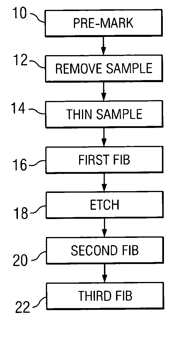
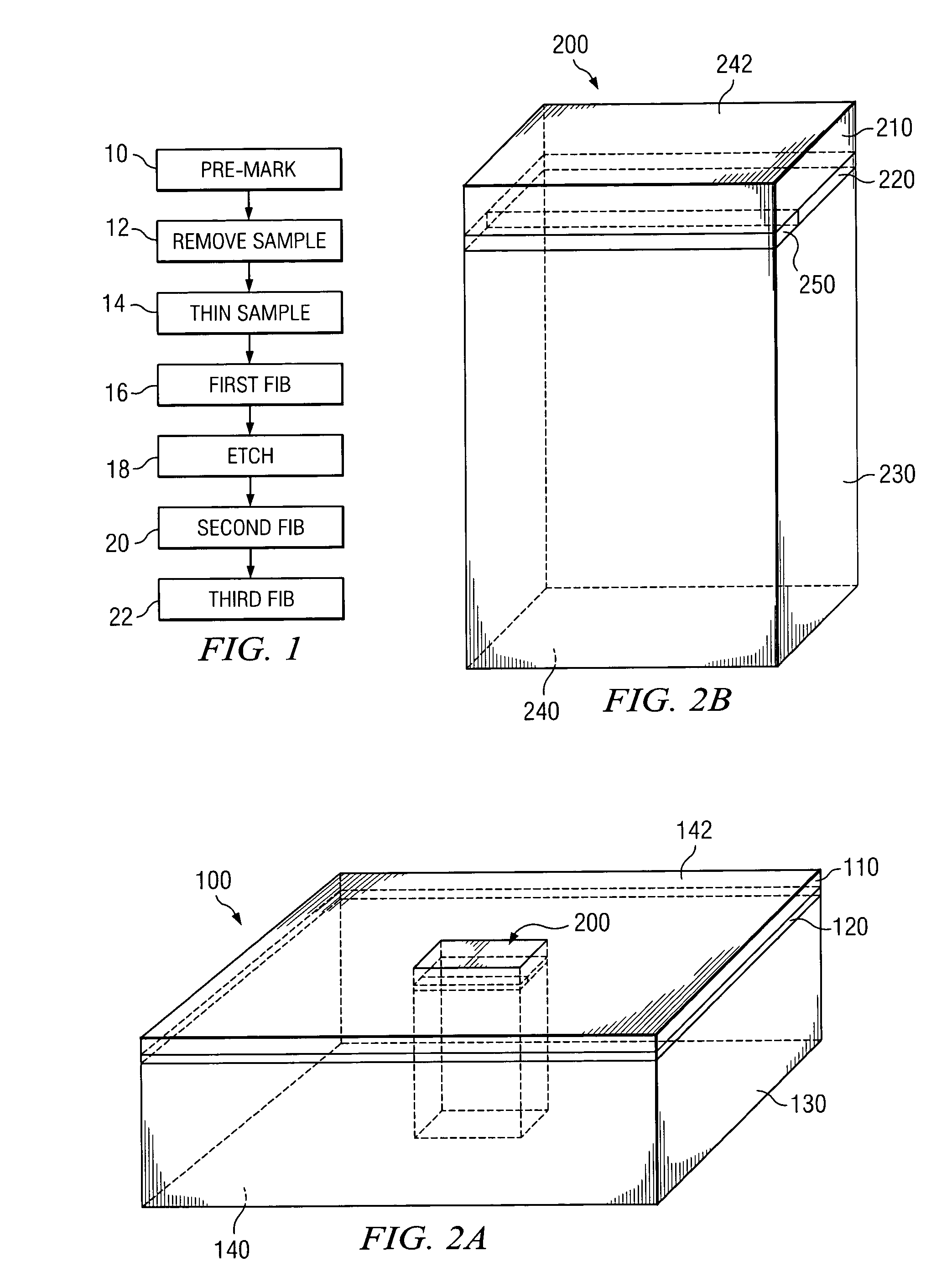
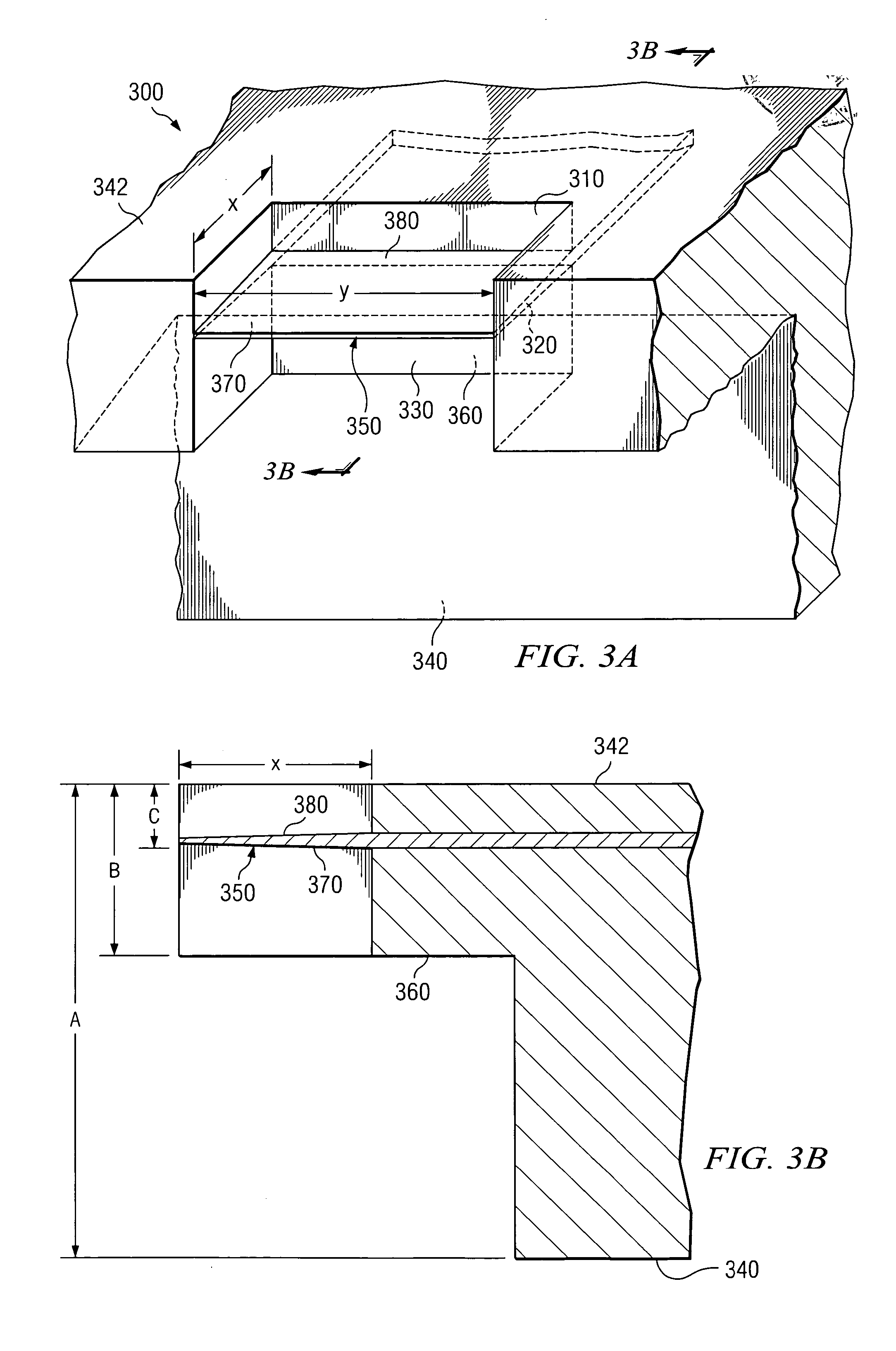
[0011] Analysis of materials using transmission electron microscopes requires that the sample analyzed should be thin enough to allow electrons to pass through it. For silicon, electron transparency is generally achieved at a thickness of approximately 0.1 μm. Semiconductor devices often contain multiple layers of materials including, for example, one or more oxide layers disposed on or between multiple polysilicon layers, all disposed on a silicon substrate. Typical semiconductors may have a thickness of 0.1 mm to 2 mm or more. Thus, significant thinning of the semiconductor device must be performed to allow for a sample of the device to be analyzed appropriately with a transmission electron microscope.

[0012] Under current techniques, samples for analysis with transmission electron microscopes (TEMs) are prepared by either thinning the area surrounding the site of interest in the sample using focused ion beam (FIB) milling or performing an etch on the site of interest to thin the ...


PUM

PropertyMeasurementUnit
thicknessaaaaaaaaaa
thicknessaaaaaaaaaa
thicknessaaaaaaaaaa

Abstract

A method for preparing a sample includes separating a portion of substrate from a sample, performing focused ion beam milling, and removing additional sample material using an etchant.

Description

TECHNICAL FIELD OF THE INVENTION [0001] This invention relates generally to the field of sample preparation and more specifically to a method for preparing a sample for transmission electron microscopy imaging and analysis. BACKGROUND OF THE INVENTION [0002] Preparing samples for plan view transmission electron microscopy generally requires the use of focused ion beam (FIB) or standard chemical etching. Standard FIB sample preparation is site specific and allows a single component of a film stack within a semiconductor device to be selected for analysis, but it suffers from sample thickness variations which limit the viewing area of the sample. Standard chemical etching is only slightly site specific, and has thickness variations that are not as severe as FIB sample preparation. With standard chemical etching, however, components from film stacks within a semiconductor device are difficult to separate, and the region surrounding the sample area is often very thin leading to mechanic...

Claims


Application Information

Patent Timeline
Patent Type & Authority Applications(United States)
IPC IPC(8): G01N1/32H01J37/305H01L21/302H01L21/461
CPCH01J37/3056G01N1/32
Inventor ANCISO, ADOLFOJONES, PATRICK J.IRWIN, RICHARD B.
Owner TEXAS INSTR INC
Why Eureka
Try Eureka