

Wide-stripe single-mode diode-laser
a diode laser and single-mode technology, applied in the direction of lasers, semiconductor laser arrangements, semiconductor lasers, etc., can solve the problems of poor quality of the output beam of the diode laser and unsuitable for applications
- Summary
- Abstract
- Description
- Claims
- Application Information
AI Technical Summary
Benefits of technology
Problems solved by technology
Method used
Image

Examples
Embodiment Construction
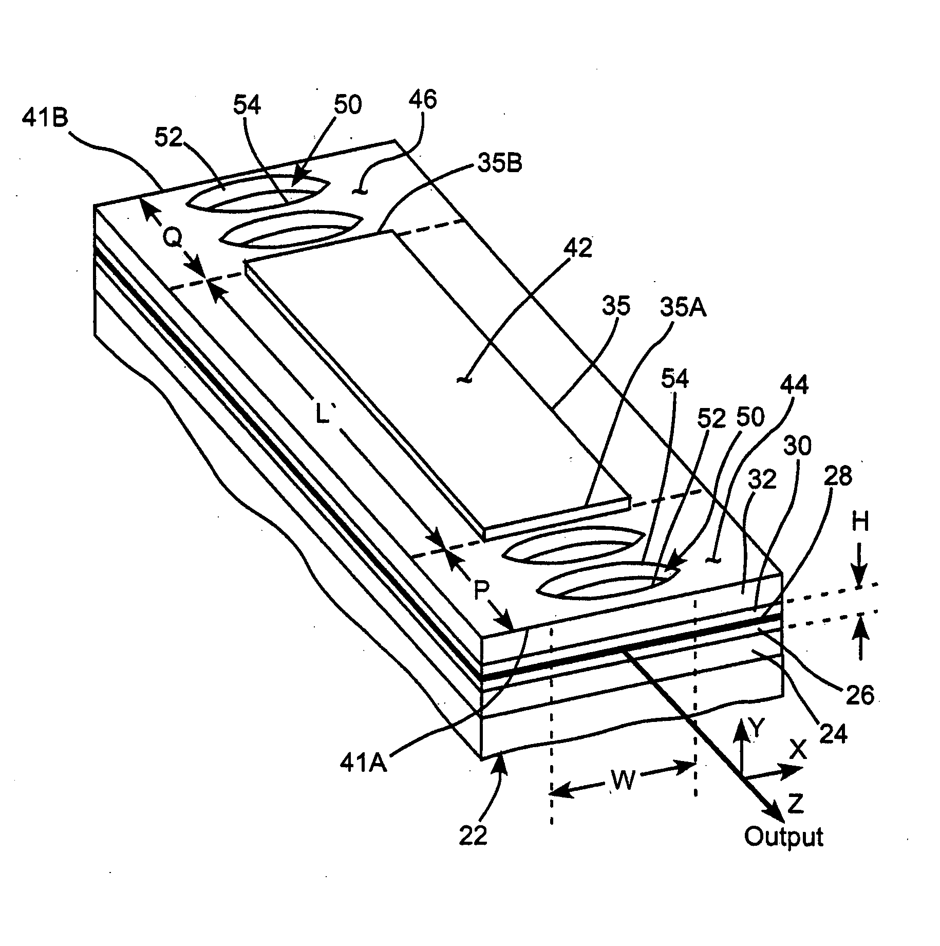
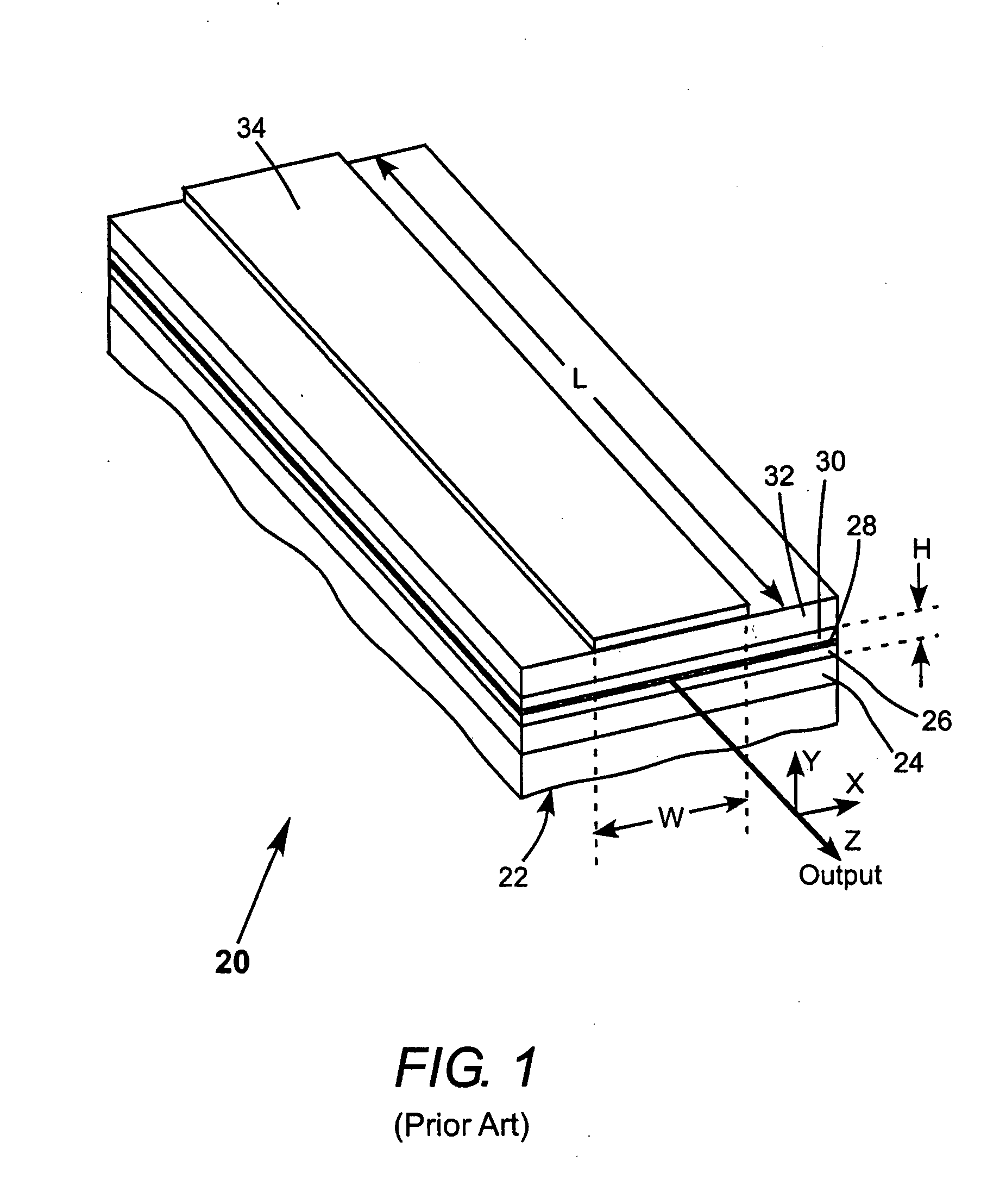
[0035] In developing wide-stripe diode-lasers in accordance with the present invention, it was determined that a significant problem in achieving single mode-operation is a thermally induced phase curvature induced in the waveguide regions due to passage of current through the diode-laser. The phase curvature results from an uneven distribution of temperature across the width, i.e., in the X-axis direction, of the diode-laser.
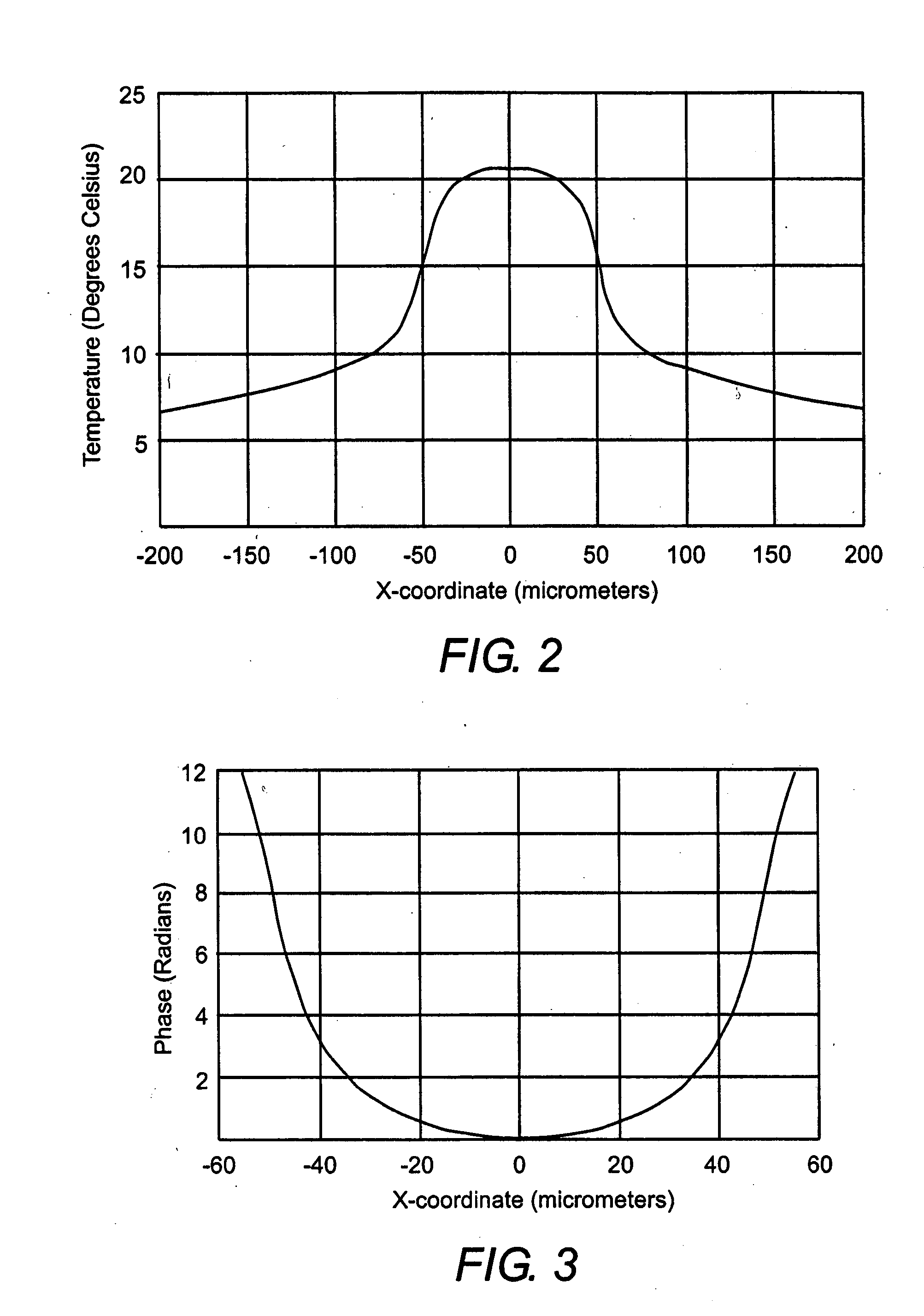
[0036] A computed, exemplary temperature distribution is schematically depicted, graphically in FIG. 2. In this calculated example, it is assumed that the diode-laser is a semiconductor structure indium-soldered to a cooper heat sink, the electrode has a width of 100 μm, and that 4 watts of current are passed through the diode-laser. The temperature peaks in the center (X=0) of the diode-laser, i.e., on the Z-axis. This temperature distribution causes a corresponding refractive index variation across the width of the diode-laser. The refractive index distribut...
PUM
 Abstract
Description
Claims
Application Information