Front substrate of plasma display panel and fabricating method thereof

a plasma display panel and front substrate technology, applied in the manufacture of electrode systems, electric discharge tubes/lamps, natural mineral layered products, etc., can solve the problems of reducing the emission efficiency of pdp and the complicated fabrication method thereof, and achieve enhanced color temperature of pdp, enhanced color purity of pdp, and enhanced contrast of pdp

Inactive Publication Date: 2005-02-24
LG ELECTRONICS INC
View PDF11 Cites 16 Cited by
  • Summary
  • Abstract
  • Description
  • Claims
  • Application Information

AI Technical Summary

Benefits of technology

[0025] An object of the present invention is to provide a front substrate of a plasma display panel and fabricating method thereof, by which a color temperature of PDP is enhanced by forming an upper dielectric layer containing a colorant amounting to a predetermined ratio for adjusting optical transmittance.
[0026] Another object of the present invention is to provide a front substrate of a plasma display panel and fabricating method thereof, by which a color purity of PDP is enhanced by forming an upper dielectric layer containing a colorant amounting to a predetermined ratio for adjusting optical transmittance.
[0027] Another object of the present invention is to provide a front substrate of a plasma display panel and fabricating method thereof, by which a contrast of PDP is enhanced by forming an upper dielectric layer containing a colorant amounting to a predetermined ratio for adjusting optical transmittance.
[0028] Another object of the present invention is to provide a front substrate of a plasma display panel and fabricating method thereof, by which PDP fabrication is simplified by forming an upper dielectric layer containing a colorant amounting to a predetermined ratio for adjusting optical transmittance.

Problems solved by technology

Specifically, as CRT (cathode ray tube) is inappropriate for the recent target of providing a large-sized and planarized screen, many efforts are made to study and develop such a flat panel display as LCD (liquid crystal display), FED (field emission display), PDP, ELD (electroluminescent display), etc.
However, the related art PDP needs to form the color filter layer on the upper dielectric layer, whereby a fabricating method thereof becomes complicated.
Yet, an aperture plane of the black stripe layer is small, whereby emission efficiency of the PDP is reduced.

Method used


Image

  • Front substrate of plasma display panel and fabricating method thereof
  • Front substrate of plasma display panel and fabricating method thereof
  • Front substrate of plasma display panel and fabricating method thereof

Examples


Embodiment Construction

[0039] Reference will now be made in detail to the preferred embodiments of the present invention, examples of which are illustrated in the accompanying drawings.

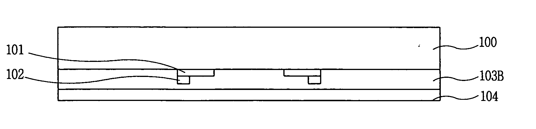
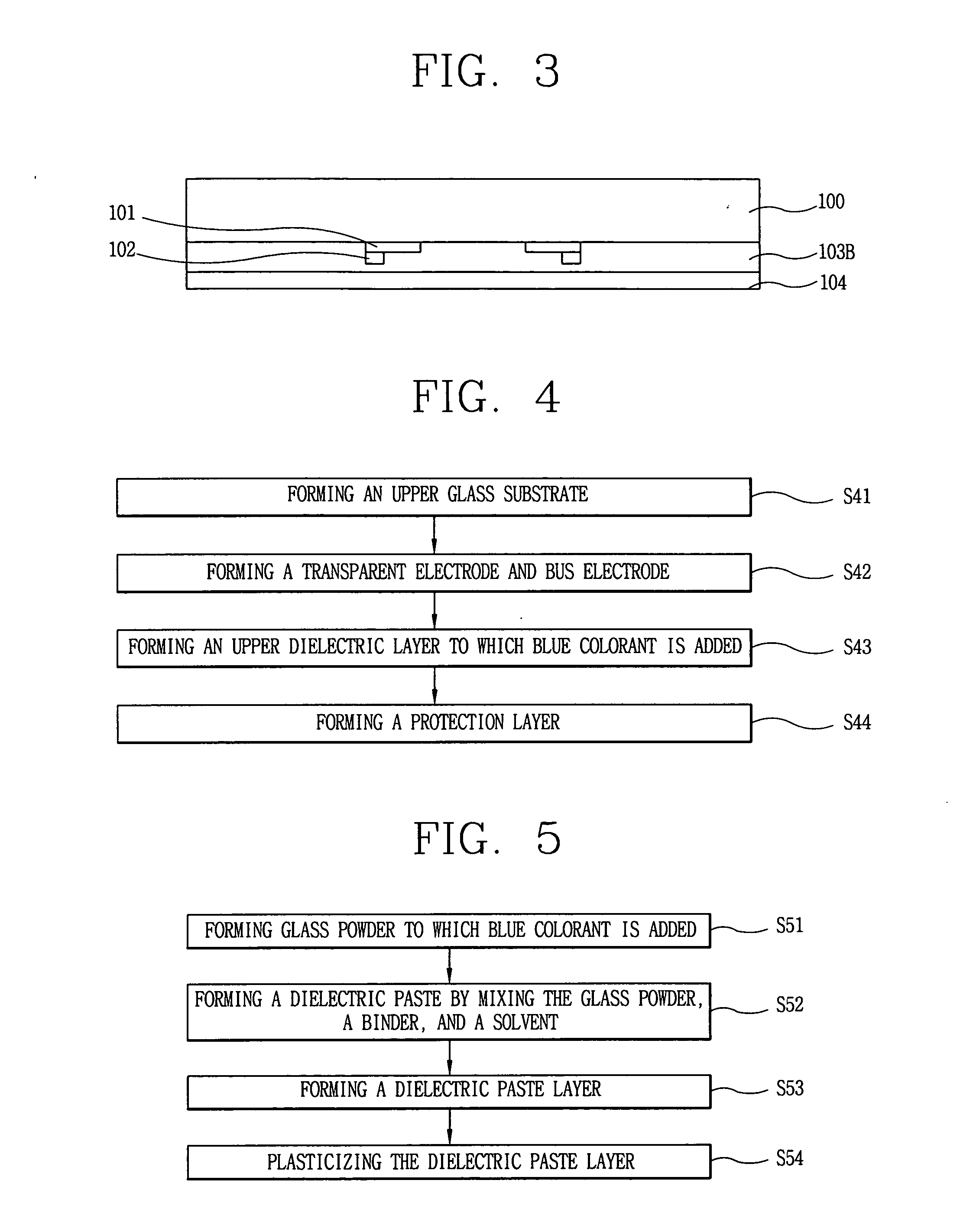
[0040]FIG. 3 is a cross-sectional view of a front substrate of PDP according to the present invention.

[0041] Referring to FIG. 3, a front substrate of PDP according to the present invention includes an upper glass substrate 100, a transparent electrode 101 and bus electrode 102 formed on the upper glass substrate 100, a colorant-added upper dielectric layer 103B formed on the upper glass substrate 100 including the transparent and bus electrodes 101 and 102 formed thereon, and a protection layer 104 formed on the upper dielectric layer 103.

[0042] A method of fabricating the above-constructed front substrate according to the present invention is explained by referring to FIG. 4 as follows.

[0043]FIG. 4 is a flowchart of a method of fabricating a front substrate of PDP according to the present invention.

[0044] Referring t...


PUM

PropertyMeasurementUnit
wt %aaaaaaaaaa
particle sizeaaaaaaaaaa
color temperatureaaaaaaaaaa

Abstract

Disclosed is a front substrate of a plasma display panel and fabricating method thereof, by which color temperature, color purity, and contrast of PDP are enhanced. The present invention includes an upper dielectric layer containing a colorant therein. And, the present invention includes the step of forming an upper dielectric layer having a colorant added thereto.

Description

BACKGROUND OF THE INVENTION [0001] 1. Field of the Invention [0002] The present invention relates to a plasma display panel (hereinafter abbreviated PDP), and more particularly, to a front substrate of a plasma display panel and fabricating method thereof. [0003] 2. Description of the Background Art [0004] Lately, a next generation multimedia display device plays a great important role as a visual information transfer means according to development and popularization of information processing systems. Specifically, as CRT (cathode ray tube) is inappropriate for the recent target of providing a large-sized and planarized screen, many efforts are made to study and develop such a flat panel display as LCD (liquid crystal display), FED (field emission display), PDP, ELD (electroluminescent display), etc. [0005] The PDP is a self-emission display device using plasma gas discharge, and has such various advantages as facilitation of size increment, excellent image quality, and fast video r...

Claims


Application Information

Patent Timeline
Patent Type & Authority Applications(United States)
IPC IPC(8): C03C8/10C03C8/08C03C8/14C03C17/04C03C17/34C03C17/36H01J9/02H01J11/22H01J11/34H01J11/38H01J11/44
CPCC03C8/14C03C17/04C03C17/3411C03C17/36Y10T428/252H01J11/12H01J11/38H01J11/44H01J2211/444C03C17/3671H01J11/40H01J9/02
Inventor LEE, SUNG WOOK
Owner LG ELECTRONICS INC
Why Eureka
Try Eureka