
Nanoscale heterojunctions and methods of making and using thereof

a technology of nanotubes and heterojunctions, applied in nanoinformatics, instruments, solid-state devices, etc., can solve the problems of reducing the electrical conductance of nanotube systems, introducing local bending, and limited control over the electrical properties of devices

Inactive Publication Date: 2005-03-03
RGT UNIV OF CALIFORNIA
View PDF6 Cites 49 Cited by
  • Summary
  • Abstract
  • Description
  • Claims
  • Application Information

AI Technical Summary

Benefits of technology

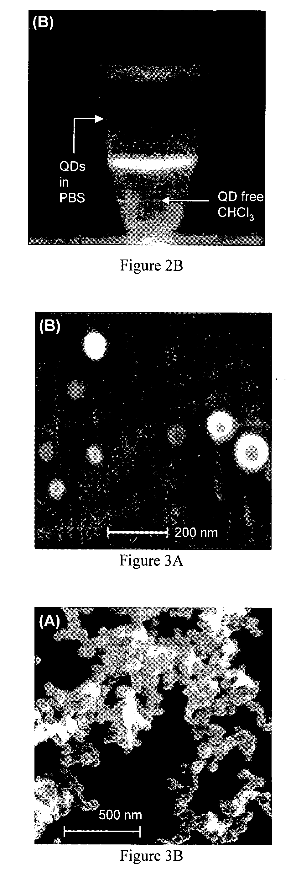
[0046]FIG. 13B shows HRTEM image of QDs in a cluster at high magnification.

Problems solved by technology

In most of the previous work on CNT based nanoscale transistors, the control over the electrical properties of the devices have been limited.
In addition, these devices relied on overlapping CNTs for forming junctions, which introduces local bending.
Distortions due to bending leads to an electron transport barrier results in reduced electrical conductance of nanotube systems.
The resulting structures from these studies indicated either undesired sidewall reactions leading to clustering of the QDs.
Sidewall functionalization adversely affects the electrical conductivity and other electronic properties of the CNT.
This is because the sidewall carbon lattices are disrupted resulting in the generation of defects along the sidewalls.
Such multiple functionalizations are yet to find practical applications in nanoelectronics.
In addition, providing contacts to a single QD for device fabrication is still one of the major challenges for nanoscale device integration.

Method used


Image

  • Nanoscale heterojunctions and methods of making and using thereof
  • Nanoscale heterojunctions and methods of making and using thereof
  • Nanoscale heterojunctions and methods of making and using thereof

Examples


Embodiment Construction

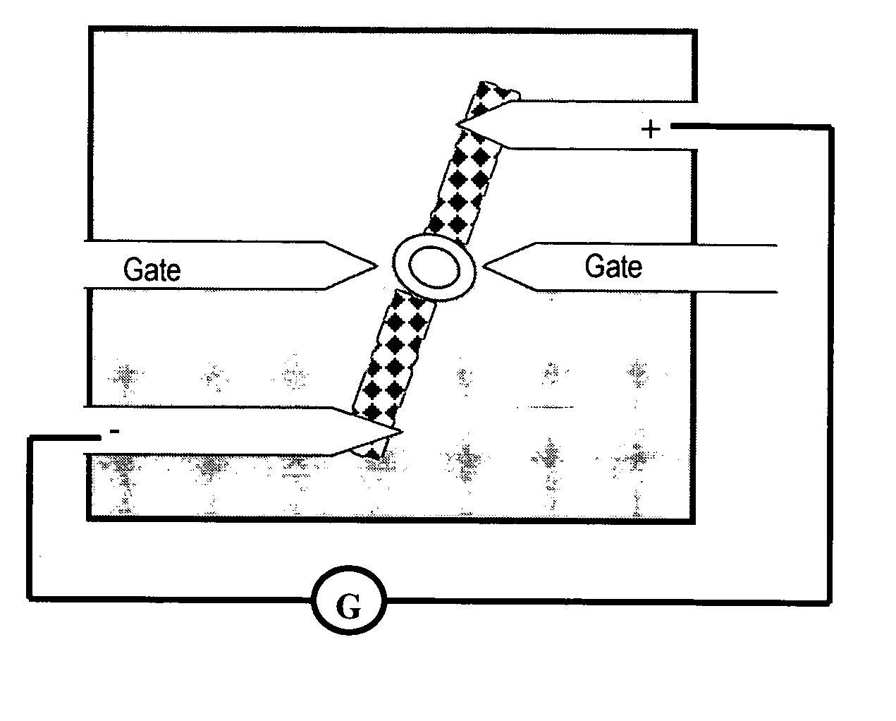
[0050] The present invention provides heterojunctions and making and using thereof. In preferred embodiments, the heterojunctions are quantum dot (CNT-QD) heterojunctions. The present invention provides methods of making the CNT-QD heterojunctions, and nanodevices comprising the CNT-QD heterojunctions.

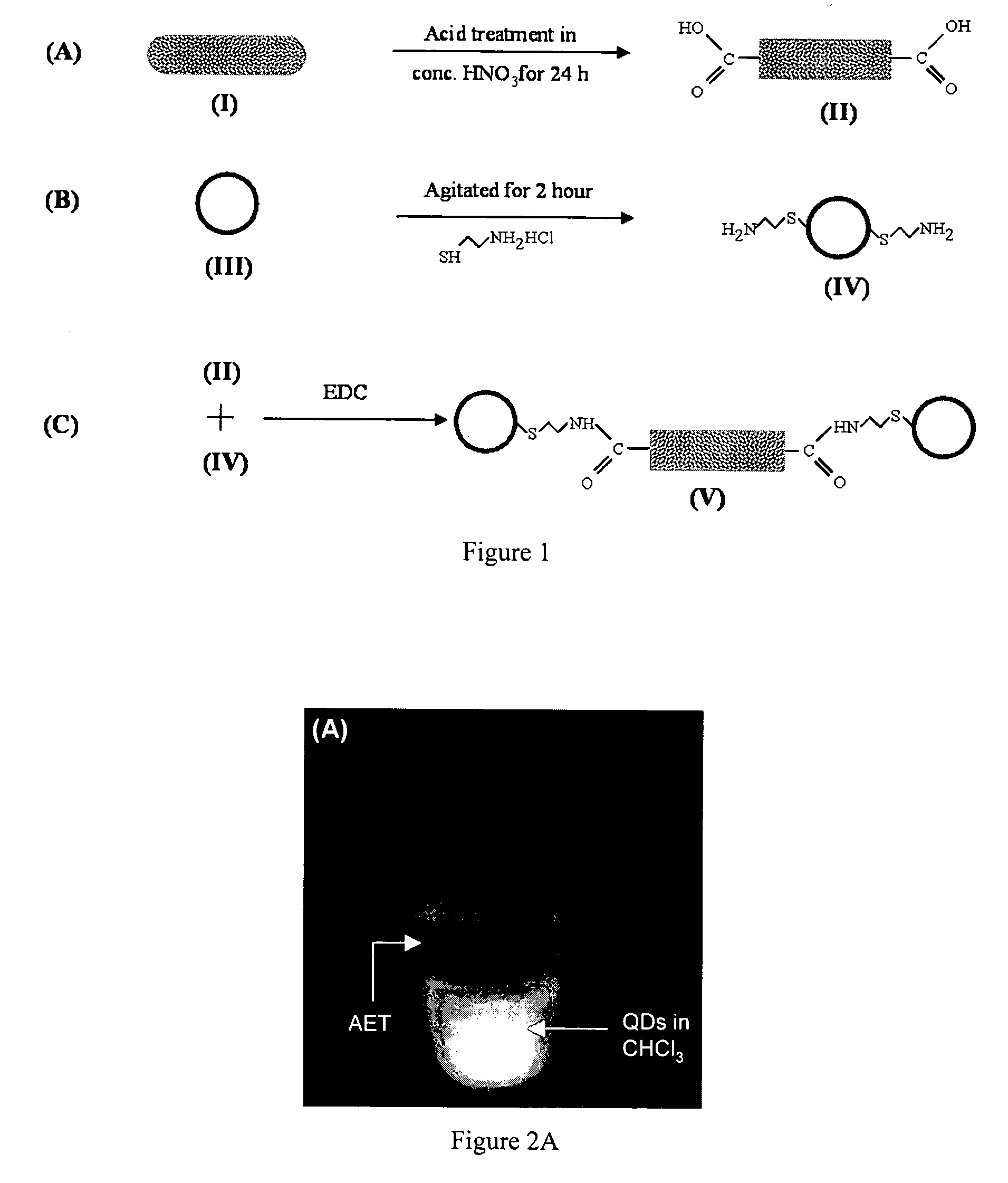
[0051] The present invention provides methods for making heterojunctions such as carbon nanotube-quantum dot (CNT-QD) heterojunctions which comprises using an ethylene carbodiimide coupling (EDC) procedure. In preferred embodiments, the present invention provides methods for the controlled synthesis of making the CNT-QD heterojunctions. The carbon nanotubes (CNTs) may be single-walled carbon nanotubes (SWCNTs) or multi-walled carbon nanotubes (MWCNTs). As used herein, CNT is used to refer to SWCNTs, MWCNTs, or both. The CNTs of the CNT-QD heterojunctions may be all SWCNTs, all MWCNT, or a mixture of both. The CNT-QD heterojunctions of the present invention may be used to connect, atta...


PUM

PropertyMeasurementUnit
lengthaaaaaaaaaa
lengthaaaaaaaaaa
lengthaaaaaaaaaa

Abstract

Disclosed herein are nanoscale heterojunctions and methods of making and using thereof. The heterojunctions comprise at least one carbon nanotube with at least one nanostructure such as a quantum dot connected, immobilized, attached, or affixed thereto. The carbon nanotubes may be single walled, multi-walled, or a combination of both. The nanostructure is preferably a quantum dot such as a ZnS capped CdSe core. The carbon nanotube heterojunctions may be employed in various nanoscale electronics and optoelectronic devices and multilayered systems including light emitting diodes, single electron transistors, spintronic devices, field emission flat panel displays, vacuum microelectronic sources, biosensors, random access memories, spin valves, and the like.

Description

CROSS REFERENCE TO RELATED APPLICATIONS [0001] This application claims the benefit of U.S. Provisional Patent Application No. 60 / 422,811, filed 30 Oct. 2002, listing Cengiz S. Ozkan as the inventor, which is herein incorporated by reference in its entirety.BACKGROUND OF THE INVENTION [0002] 1. Field of the Invention [0003] The present invention generally relates to nanoscale heterojunctions and methods of making and using thereof. [0004] 2. Description of the Related Art [0005] The unique electrical, mechanical, and chemical properties of carbon nanotubes have made them intensively studied materials in the field of nanotechnology. See Dai, H. J. (2002) Surface Sci. 500:218; Ajayan, P. M. (1999) Chem. Rev. 99:1787; Yakobson, B. I. and Smalley, R. E. (1997) Am. Sci. 85:324; and Dresselhaus, M. S., et al. (1996) Science of Fullerenes and Carbon Nanotubes; Academic Press, New York, which are herein incorporated by reference. A number of device applications of these nanoscale materials h...

Claims


Application Information

Patent Timeline
Patent Type & Authority Applications(United States)
IPC IPC(8): G11C13/02H01L21/00H01L29/06H01L29/12H01L29/22H01L51/05H01L51/30
CPCB82Y10/00G11C13/025G11C2213/17H01L29/0665H01L29/0673H01L51/0595H01L29/127H01L29/22H01L51/0048H01L51/0508H01L51/0587H01L29/068H10K85/221H10K10/46H10K10/29H10K10/701
Inventor OZKAN, CENGIZ S.RAVINDRAN, SATHYAJITHLAKE, ROGEROZKAN, MIHRIMAHPORTNEY, NATAN
Owner RGT UNIV OF CALIFORNIA
Learn More