Integrated circuit package having an inductance loop formed from a multi-loop configuration

a multi-loop configuration and integrated circuit technology, applied in the field of integrated circuits, can solve the problems of increasing the risk of damage to the integrated circuit, increasing the cost and complexity of the manufacturing process, and many integrated circuits are not self-contained devices, so as to achieve fewer processing steps to manufacture and more economical

Inactive Publication Date: 2005-03-03
GCT SEMICONDUCTOR INC
View PDF22 Cites 18 Cited by
  • Summary
  • Abstract
  • Description
  • Claims
  • Application Information

AI Technical Summary

Benefits of technology

An object of the present invention is to provide an integrated circuit package which is more economical and requires fewer processing steps to manufacture than conventional IC packages.

Problems solved by technology

Many integrated circuits are not self-contained devices.
The need to establish off-package connections increases the cost and complexity of the manufacturing process and therefore is considered highly undesirable.
These connections also expose the integrated circuit to an increased risk of damage from external influences, which translate into degradation in reliability and performance.
The use of off-package or board-mounted inductors increases system costs.
Moreover, connection problems may occur between the package and board which may adversely affect the reliability and performance of the PLL circuitry.
The approach taken in the '735 patent is undesirable for at least two reasons.
The need to form these special pads increases the cost and complexity of the manufacturing process.
Second, in order to accommodate the bonding pads, the size of the integrated circuit substrate must be increased and as a result more circuit board space is consumed.
These effects undermine the goal of increasing integration and miniaturization.
While this approach does not require the formation of special bonding pads on the package substrate, it is has at least two drawbacks that make it undesirable.
As previously noted, these wires are susceptible to damage during manufacture and / or use.
This is undesirable because the wire could short certain portions of the chip circuitry and introduce noise and other interfering influences which substantially degrade chip performance.

Method used


Image

  • Integrated circuit package having an inductance loop formed from a multi-loop configuration
  • Integrated circuit package having an inductance loop formed from a multi-loop configuration
  • Integrated circuit package having an inductance loop formed from a multi-loop configuration

Examples


Embodiment Construction

The present invention is, in one respect, a semiconductor package having an integrated circuit chip and an inductor loop which is connected in a self-contained manner within the package. The present invention is also a system which is at least partially controlled by the inductor loop of the semiconductor device mentioned above. The system may be a communications system where the inductor loop is used to set a transmitter and / or RF carrier frequency or another type of system. The various embodiments of the invention will now be discussed in seriatim below.

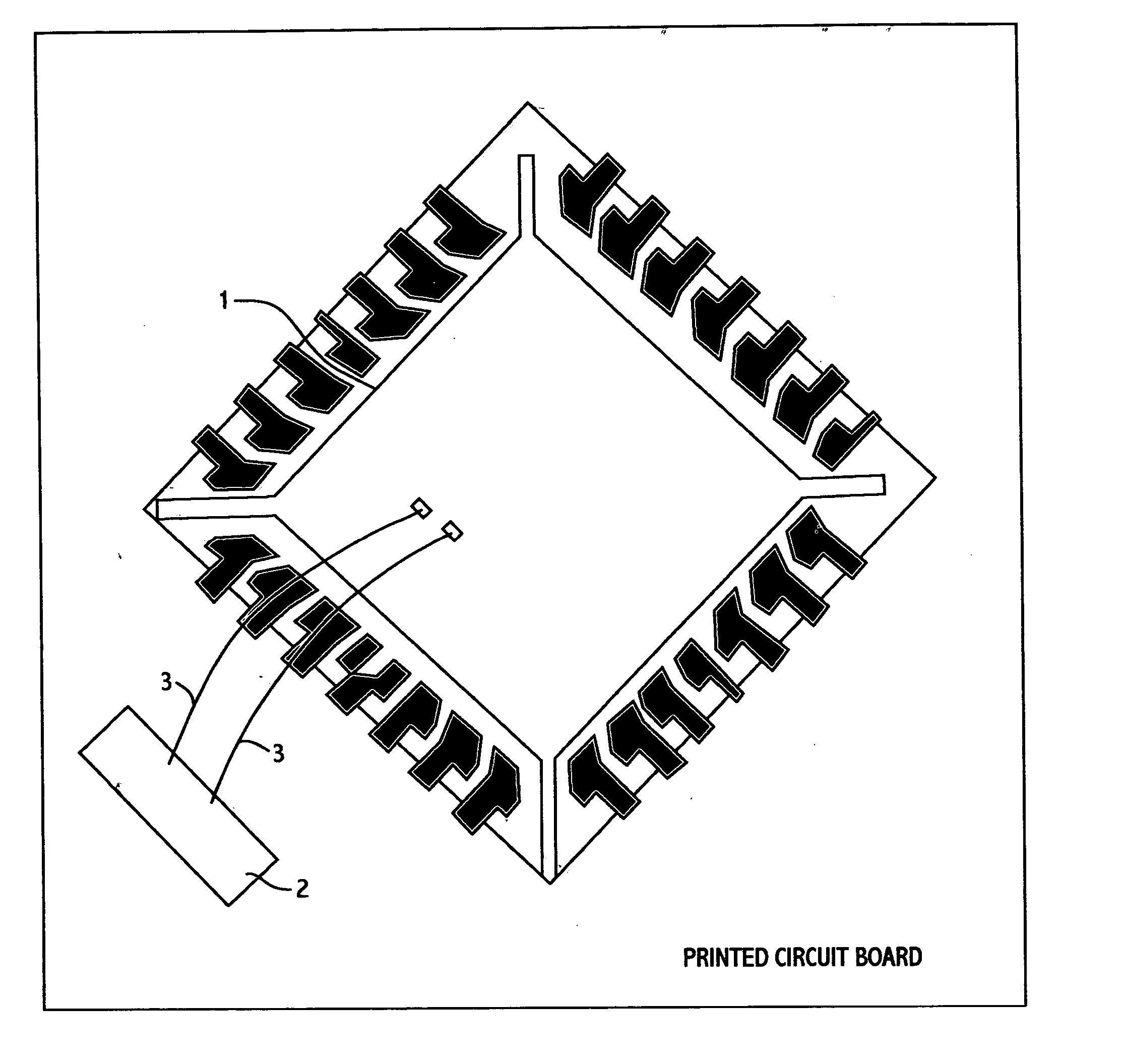
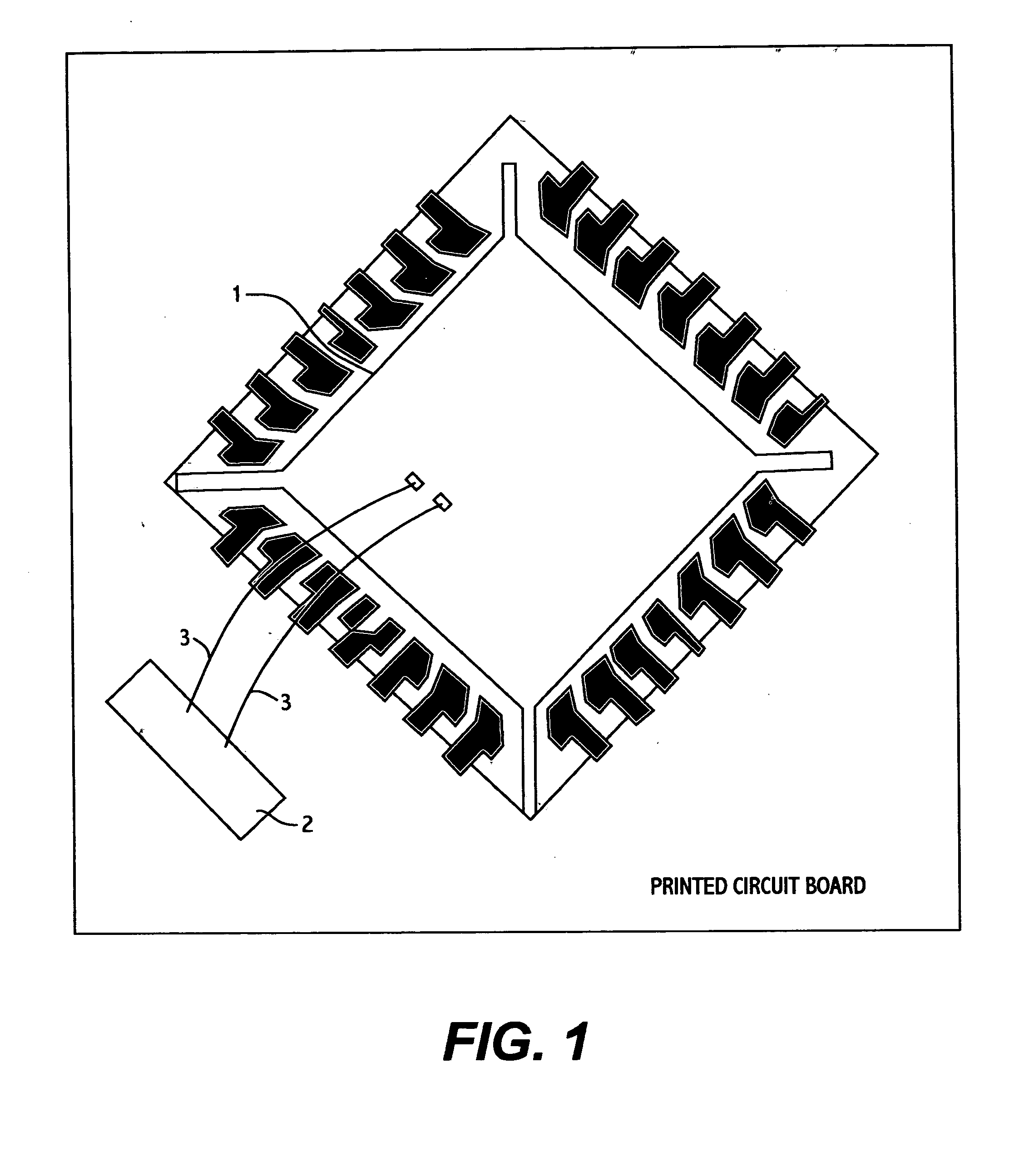
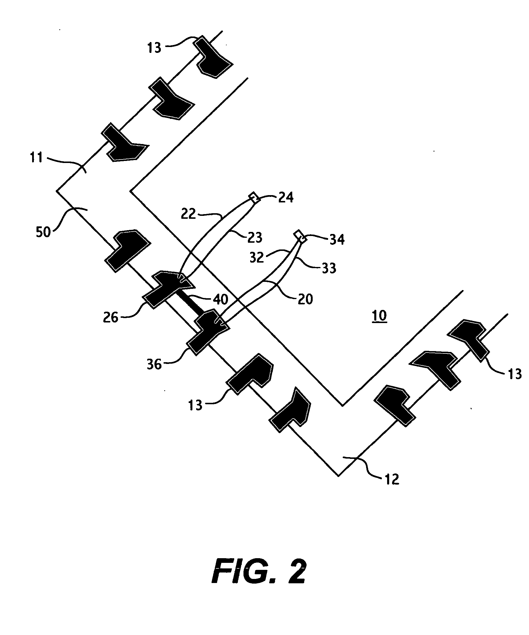
FIG. 2 shows a semiconductor package in accordance with a first embodiment of the present invention. This package includes an integrated circuit chip 10 mounted on or within a package housing 11. The housing includes a substrate 12 for supporting the chip and a plurality of input / output (I / O) pins 13 formed on the substrate for electrically connecting the chip to one or more external circuits (not shown). The substrate may be any...


PUM


Abstract

An integrated circuit package includes an inductance loop formed from a connection of lead wires and one or more input/output (I/O) package pins. In one embodiment, the inductance loop is formed from first and second wires which connect a first bonding pad on the integrated circuit chip to a first I/O pin of the package and a third and fourth wires which connect a second bonding pad on the chip to a second I/O pin of the package. To complete the inductor loop, the first and second I/O pins are connected by a third conductor between the pins. The third conductor may include one or more bonding wires and the I/O pins are preferably ones which are adjacent one another. However, the loop may be formed from non-adjacent connections of I/O pins based, for example, on loop-length requirements, space considerations, and/or other design or functional factors. In another embodiment, connection between the first and second I/O pins is established by making the I/O pins have a unitary construction. In another embodiment, connection between the first and second I/O pins is established by a metallization layer located either on the surface of the package substrate or within this substrate. By forming the inductor loop within the limits of the integrated circuit package, a substantial reduction in space requirements is realized, which, in turn, promotes miniaturization. Also, the integrated circuit may be implemented in any one of a variety of systems, at least one parameter of which is controlled by the length of the inductor loop of the package.

Description

BACKGROUND OF THE INVENTION 1. Field of the Invention This invention generally relates to integrated circuits, and more particularly to an integrated circuit package having an inductance loop formed from at least one input / output pin of the package. The invention also relates to a system which is at least partially controlled by the inductor loop of the package. 2. Description of the Related Art One perennial goal among circuit designers is to decrease the size of integrated circuits. This goal is largely driven by market demand for ever-smaller consumer electronics, communications devices, and display systems to mention a few. There are, however, a number of impediments that undermine this goal, one of which will now be discussed. Many integrated circuits are not self-contained devices. To ensure proper operation, these circuits must therefore be connected to one or more external components through connections which do not involve the use of an IC package input / output pin. Thi...

Claims


Application Information

Patent Timeline
Patent Type & Authority Applications(United States)
IPC IPC(8): H01LH01L23/64H01L29/00
CPCH01L23/642H01L2924/014H01L24/49H01L2224/48091H01L2224/49111H01L2224/49113H01L2924/01005H01L2924/01006H01L2924/01013H01L2924/01033H01L2924/01078H01L2924/01082H01L2924/14H01L2924/15192H01L2924/19041H01L2924/19042H01L2924/19043H01L2924/30105H01L2924/30107H01L23/645H01L2924/01076H01L24/48H01L2924/01019H01L2924/01023H01L2924/01043H01L2924/00014H01L2224/05553H01L2224/45099H01L2224/05599H01L23/495
Inventor KOO, YIDOHUH, HYUNGKILEE, KANG YOONLEE, JEONG-WOOPARK, JOONBAELEE, KYEONGHO
Owner GCT SEMICONDUCTOR INC
Why Eureka
Try Eureka