

Semiconductor device
a semiconductor and shielding technology, applied in the details of semiconductor/solid-state devices, semiconductor devices, electrical apparatus, etc., can solve the problems of increasing the size of semiconductor devices, affecting the spiral inductor by noise and unnecessary signals, and affecting so as to achieve the effect of not impairing the flexibility of wiring layou
- Summary
- Abstract
- Description
- Claims
- Application Information
AI Technical Summary
Benefits of technology
Problems solved by technology
Method used
Image

Examples
embodiment 1
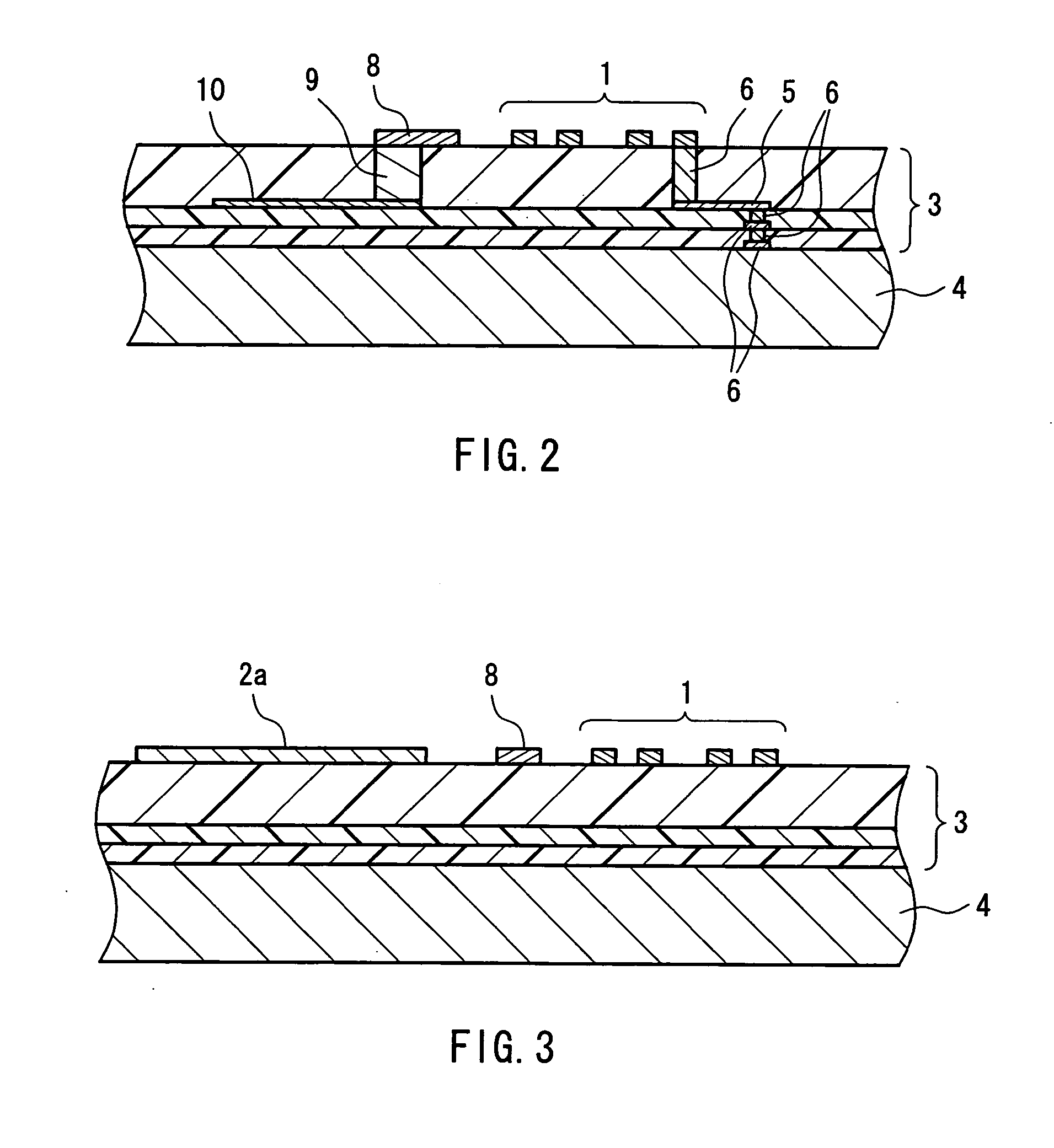
[0025] FIGS. 1 to 3 show a semiconductor device according to Embodiment 1. FIG. 1 is a top plan view of the semiconductor device. FIG. 2 is a cross-sectional view taken along line A-A′ of FIG. 1 and FIG. 3 is a cross-sectional view taken along line B-B′ of FIG. 1. In the following descriptions, the same reference numerals are assigned to the same elements as those in the conventional example.
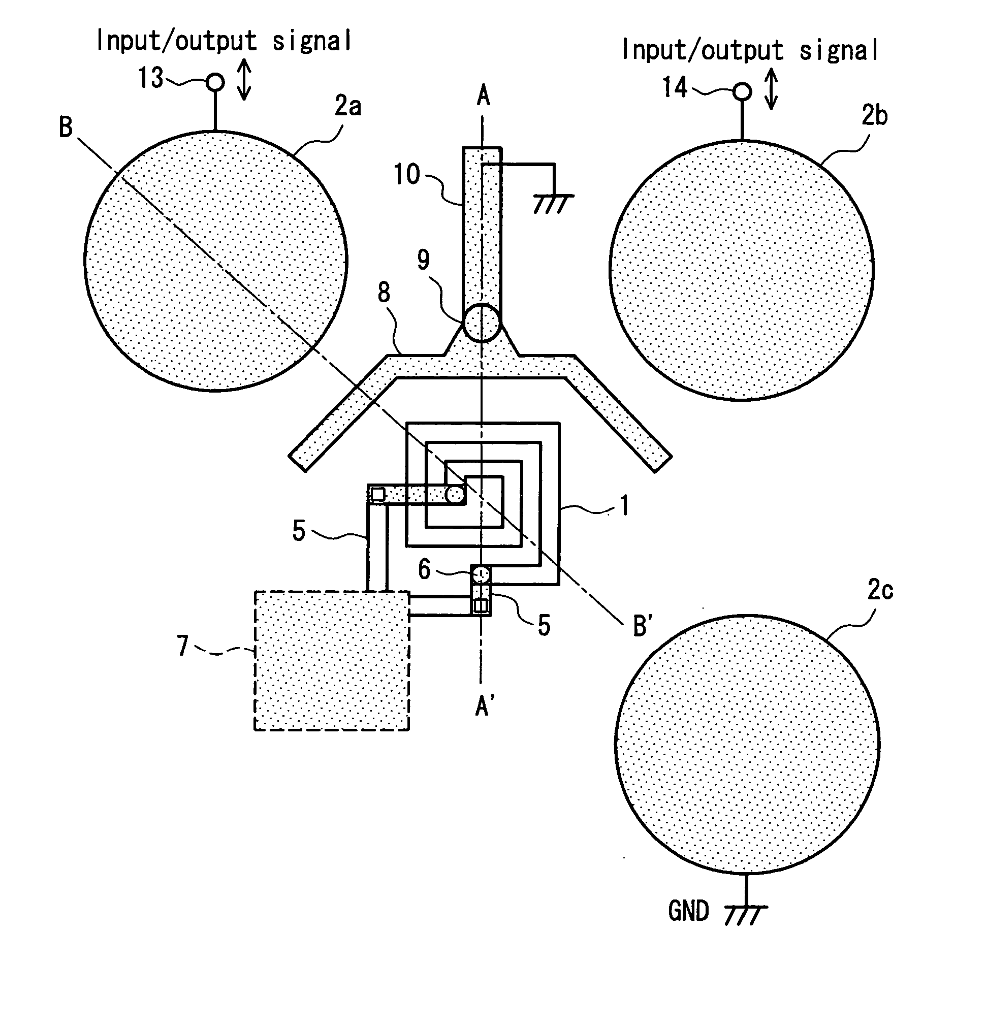
[0026] In FIG. 1, reference numeral 1 denotes a spiral inductor, around which connection terminals 2a, 2b and 2c leading to a printed board or the like are disposed. The connection terminals 2a and 2b each are connected with input / output terminals 13, 14 for an electrical signal, and the connection terminal 2c is connected with the ground. The spiral inductor 1 is connected with a circuit block 7 by way of a wiring 5 and a via 6 for the interlayer connection of the wiring layer.
[0027] As shown in FIG. 2, the wiring 5 and the via 6 are formed at a multilayered wiring region 3 including a wiring...
embodiment 2
[0031]FIG. 4 is a top plan view of a semiconductor device according to Embodiment 2 of the present invention. The same reference numerals are assigned to the same elements as those of Embodiment 1 shown in FIG. 1 so as to simplify the explanations.
[0032] In the present embodiment, as shown in FIG. 4, a spiral inductor 1 and a spiral inductor 11 are arranged to be symmetric with respect to a line. The spiral inductors 1 and 11 are connected with a differential circuit. In the vicinity of the spiral inductor 11, connection terminals 2d and 2e are disposed, through which connection with an external terminal of the semiconductor device is established. Between the spiral inductor 11 and the connection terminals 2d and 2e, a shielding wiring pattern 12 is disposed. The connection terminal 2d is connected with an electrical signal input / output terminal 15, and the connection terminal 2e is connected with the ground and also with the shielding wiring pattern 12.
[0033] The present embodime...
embodiment 3
[0036]FIG. 5 is a block diagram of radio equipment according to Embodiment 3 of the present invention. The present embodiment shows one example in which the combination of the spiral inductor and the shielding wiring pattern that are configured similarly to the above-described embodiments is applied to a semiconductor device 27 constituting a part of the radio equipment.
[0037] A signal is input from the outside to the semiconductor device 27 by way of an antenna 21, a transfer switch 22, a low noise amplifier 23, a filter 24, a power amplifier 25 and a filter 26, and a signal is output to the outside from the semiconductor device 27. The semiconductor device 27 is made up of an amplifier 28, a gain control amplifier 29, a mixer 30, a local part 31, a base band processing part 32 and the like. The semiconductor device 27 performs input / output of signals with respect to a control processing part 33. The control processing part 33 is connected with a display part 34, an input part 35,...
PUM
 Abstract
Description
Claims
Application Information