Electronic control apparatus
- Summary
- Abstract
- Description
- Claims
- Application Information
AI Technical Summary
Benefits of technology
Problems solved by technology
Method used
Image

Examples
first embodiment
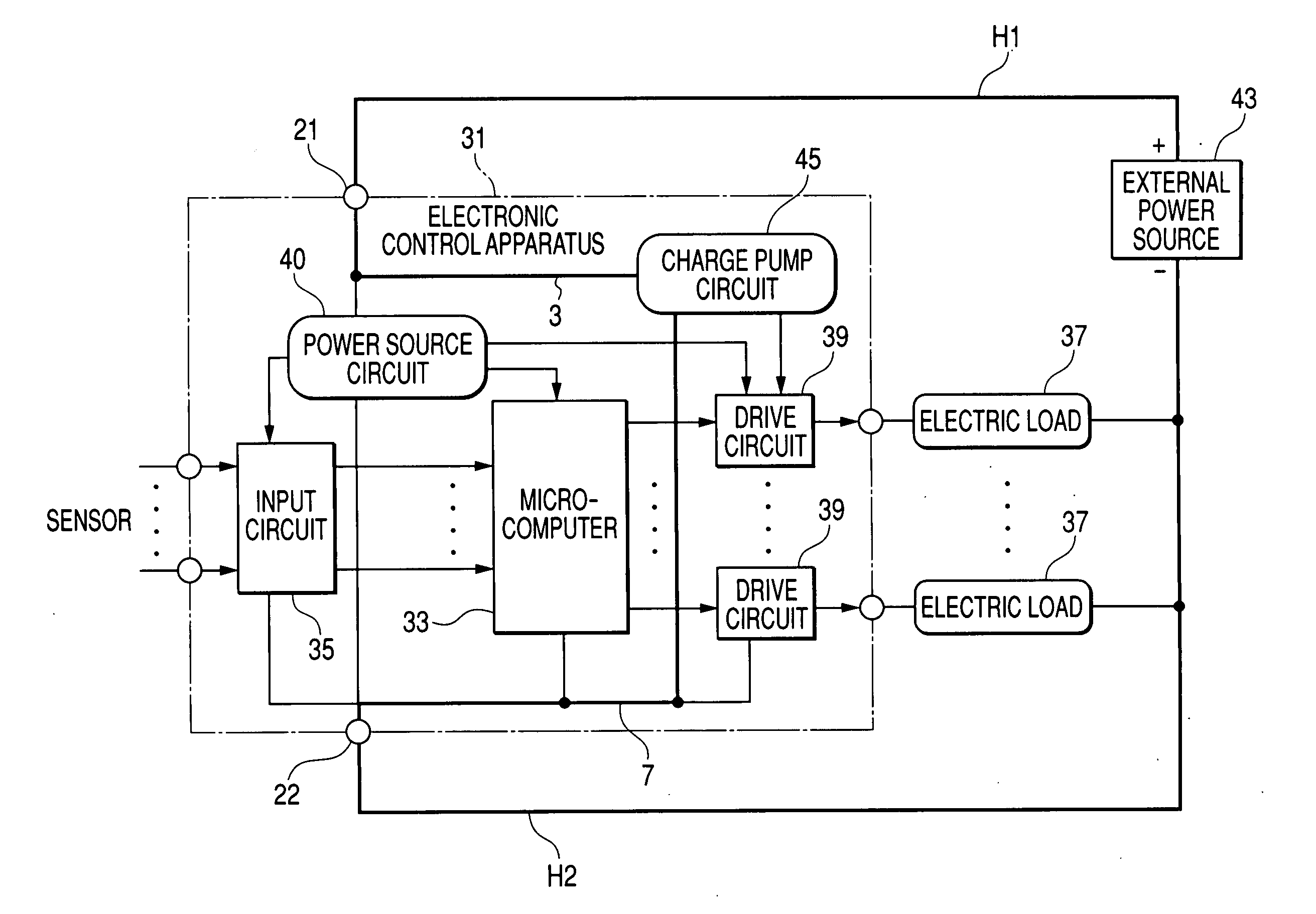
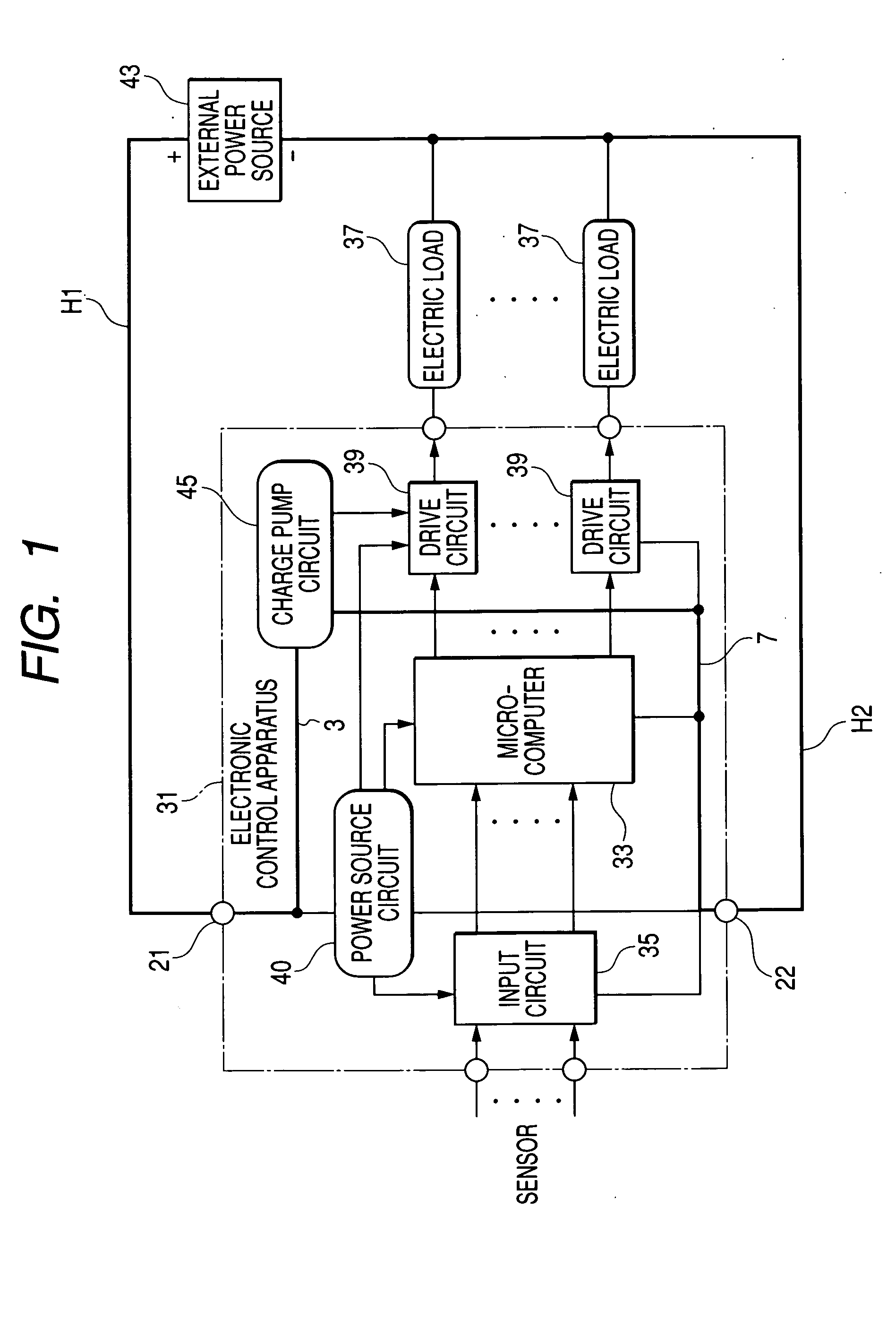
[0079] In view of the foregoing, the present invention provides an electronic control apparatus as described hereinafter. FIG. 1 is a circuit diagram showing the schematic arrangement of an electronic control apparatus 31 in accordance with the present invention, which is installed in an automotive vehicle.
[0080] As shown in FIG. 1, the electronic control apparatus 31 according to the first embodiment includes a microcomputer 33, an input circuit 35, a plurality of load drive circuits 39, and a power source circuit 40. The input circuit 35 receives sensor signals of various sensors, applies the filter processing to these signals, and supplies the filtered sensor signals to the microcomputer 33. The apparatus 31 is connected to a plurality of electric loads 37 which are provided outside this apparatus 31. Each load drive circuit 39 receives a command signal from the microcomputer 33 and drives a corresponding electric load 37 in accordance with the command signal. An external power s...
second embodiment
[0109] Furthermore, the common power source wiring 3 is formed in the third layer of the printed board 49. The third layer is second closest to the surface layer (i.e. uppermost layer) of the printed board 49 (in other words, highest but two) as shown in FIG. 7. The common power source wiring 3 is connected via the via-hole va to the power source wiring Pp1 of the surface layer. Similarly, the common ground wiring 7 is formed in the fifth layer of the printed board 49. The fifth layer is fourth closest to the surface layer (i.e. uppermost layer) of the printed board 49 (in other words, highest but four) as shown in FIG. 7. The common ground wiring 7 is connected via the via-hole vb to the ground wiring Pg1 of the surface layer.
[0110] The power source wiring Pp1 of the surface layer (corresponding to the power source wiring 2 shown in FIGS. 2 and 3) connects the via-hole va to the power source wiring 1. The ground wiring Pg1 of the surface layer (corresponding to the ground wiring 6...
third embodiment
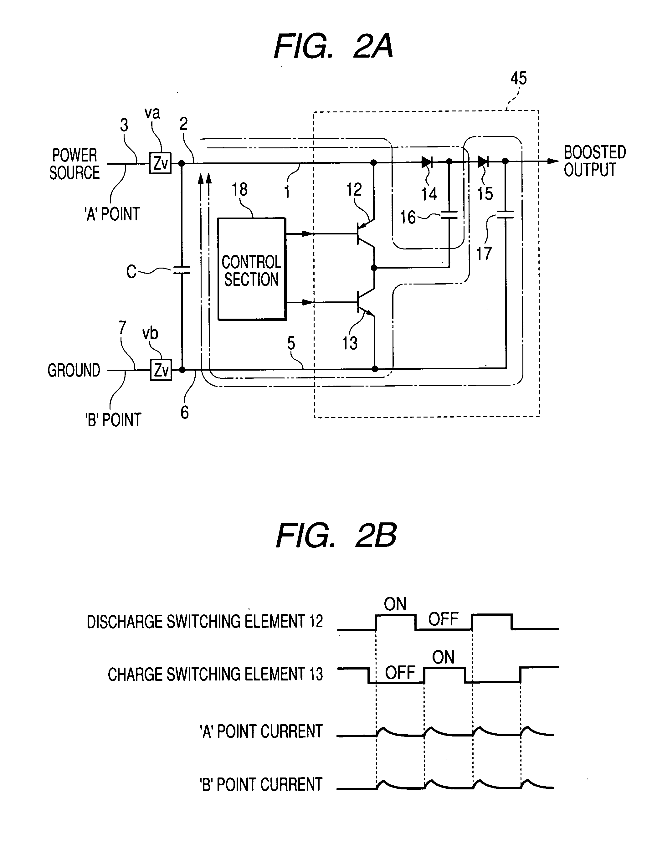
[0115] As shown in FIG. 8, the common power source wiring 3 is connected to the exclusive power source wiring 1 of the charge pump circuit 45 via a through-hole 55. A lead terminal 53A of the lead component 53 is inserted or embedded in the through-hole 55. Especially, the lead component 53 is different from the components arranging the capacitor C and the charge pump circuit 45 and is not adversely influenced by the current changes occurring in the power source wiring.
[0116] According to the third embodiment, it is not necessary to provide any special via hole for connecting the power source wiring 1 to the common power source wiring 3. This is advantageous in realizing the space-saving and the cost-reduction of the printed board 51.
[0117]FIG. 8 omits the depiction of the exclusive ground wiring 5 for the charge pump circuit 45. However, it will be readily understood that the ground wiring 5 and the common ground wiring 7 are connected via a through-hole in which a lead terminal ...
PUM
 Abstract
Description
Claims
Application Information
 - R&D Engineer
- R&D Manager
- IP Professional
- Industry Leading Data Capabilities
- Powerful AI technology
- Patent DNA Extraction
Browse by: Latest US Patents, China's latest patents, Technical Efficacy Thesaurus, Application Domain, Technology Topic.
© 2024 PatSnap. All rights reserved.Legal|Privacy policy|Modern Slavery Act Transparency Statement|Sitemap