EEPROM device and method for providing lower programming voltage

Active Publication Date: 2005-03-03
TEXAS INSTR INC
View PDF1 Cites 3 Cited by
  • Summary
  • Abstract
  • Description
  • Claims
  • Application Information

AI Technical Summary

Benefits of technology

[0010] In accordance with an exemplary embodiment, an exemplary method for providing a lower programming voltage in an EEPROM device comprises the steps of modifying a mask drawing layer with one or more serrat

Problems solved by technology

Non-distributive or other standard EEPROM devices require expensive process step changes and modifications during manufacturing.
As a result, an analog circuit using an EEPROM device for calibration can only be calibrated or trimmed typically during probe or final test operation at the manufacturer's location, as opposed to after packaging and / or after customer printed circuit board mounting.
In addition, current precision analog integrated circuits have become very susceptible to physical stress mis-calibration, such as that occurring after final testing at the manufacturer's location.
For example, since silicon is a piezoelectric material, any strain placed on the silicon, whether from the plastic packaging or from mounting the integrated circuit to the printed circuit board, often results in mis-calibration.
However, standard distributive EEPROM devices generally require approximately 10 volts for programming of a 5V CMOS analog circuit, making such EEPROM devices unsuitable for programming by on-chip devices.

Method used


Image

  • EEPROM device and method for providing lower programming voltage
  • EEPROM device and method for providing lower programming voltage
  • EEPROM device and method for providing lower programming voltage

Examples


Embodiment Construction

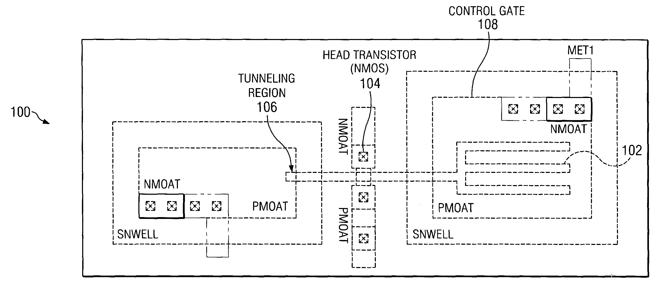
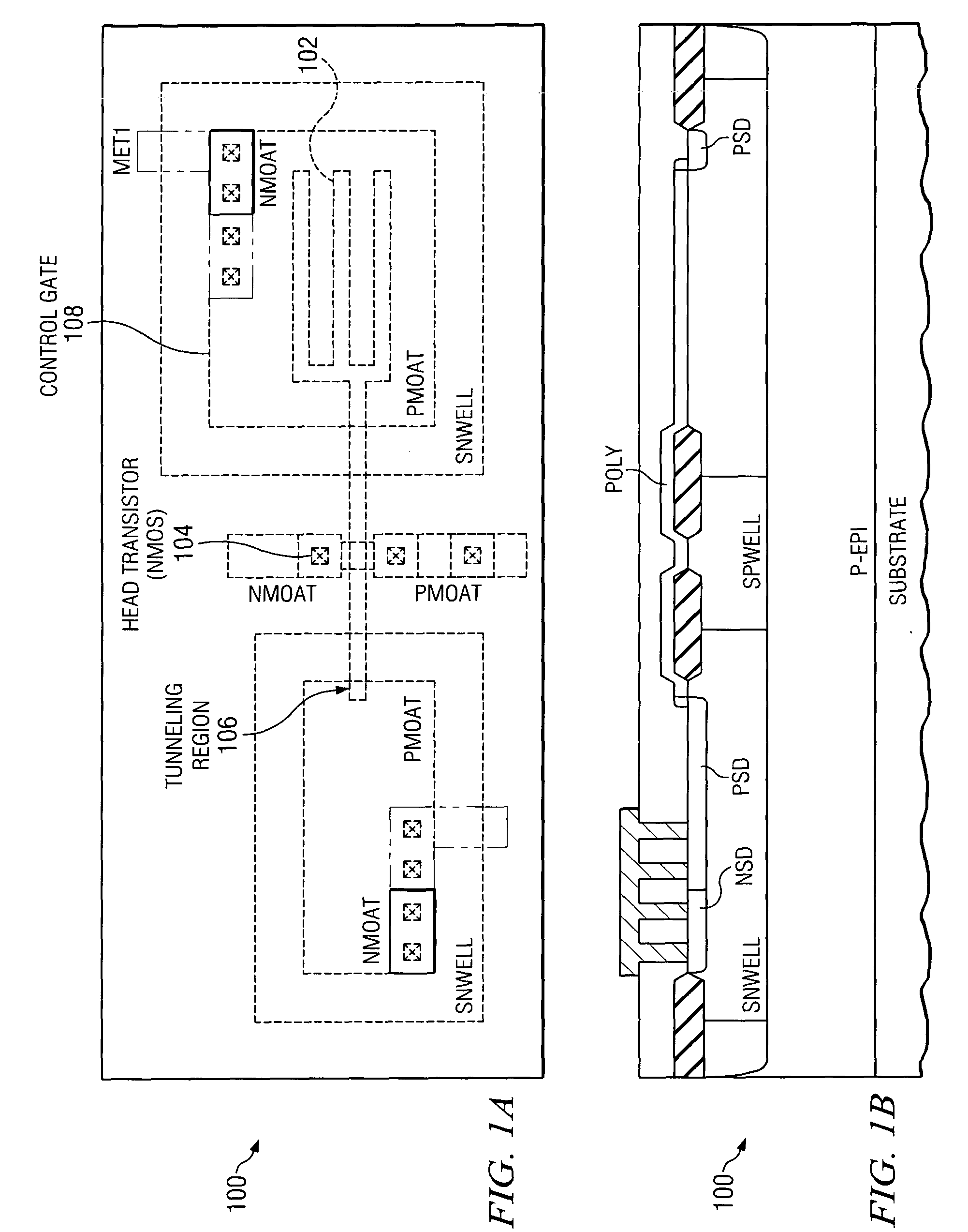
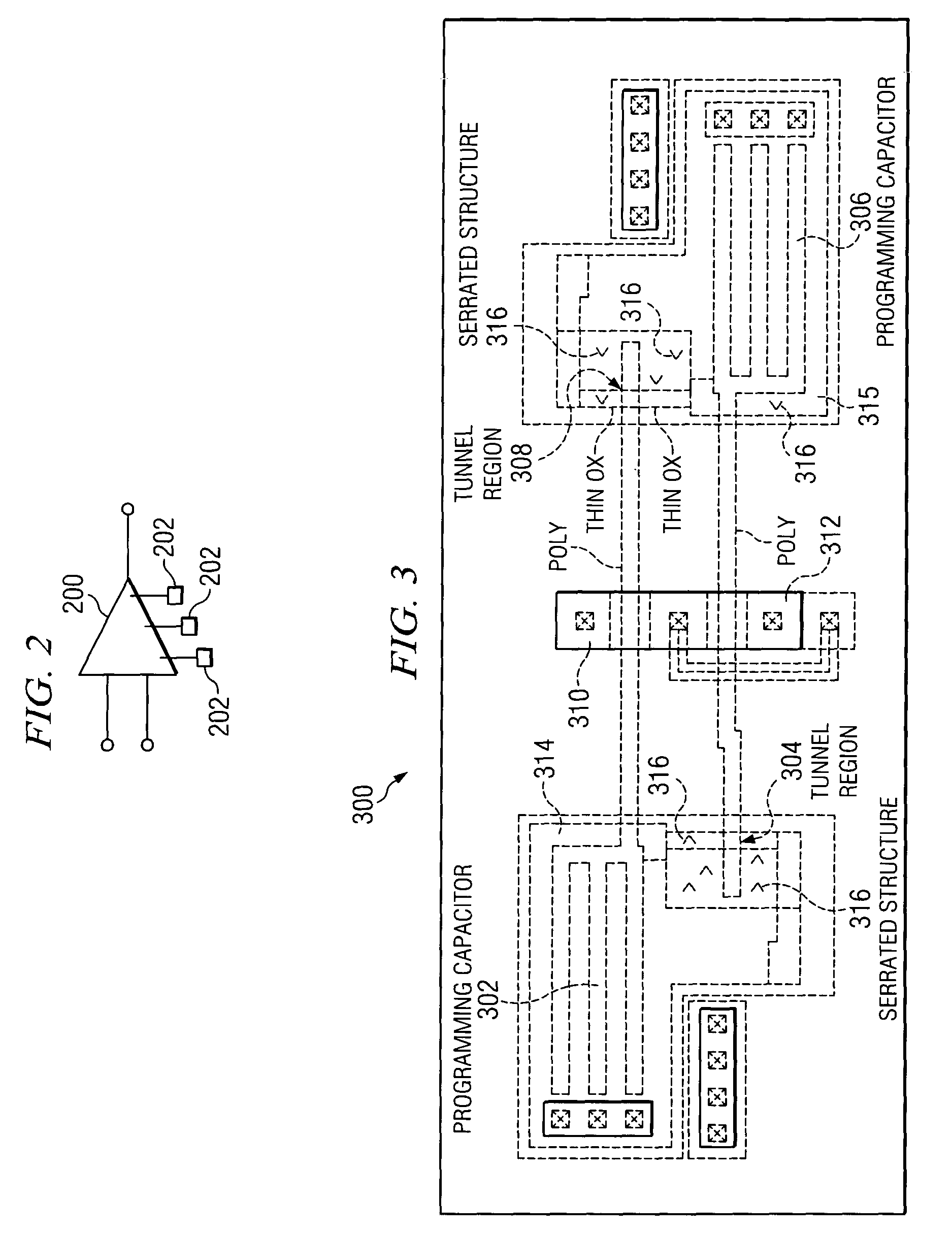
[0019] The present invention may be described herein in terms of various functional components. It should be appreciated that such functional components may be realized by any number of hardware or structural devices configured to perform the specified functions. For example, the present invention may employ various integrated components, e.g., buffers, supply references, current sources, signal conditioning devices and the like, comprised of various electrical devices, e.g., resistors, transistors, capacitors, diodes and other components whose values may be suitably configured for various intended purposes. In addition, the present invention may be practiced in any integrated circuit application where a restriction of growth of gate oxide can be utilized. However, for purposes of illustration only, exemplary embodiments of the present invention are described herein in connection with an EEPROM device application, such as for calibration or operation within an analog circuit. Furthe...


PUM


Abstract

An improved EEPROM device and method for providing a lower device programming voltage is disclosed. An exemplary EEPROM device is configured with a modified drawing layer comprising one or more serrated elements configured underneath a tunneling region of the EEPROM device. The serrated elements can comprise regions having at least one acute angle structure within the active mask drawing layer configured to provide a restriction of the oxygen used to grow the gate oxide that determines the programming voltage of the EEPROM device. In addition the serrated elements can also be configured with at least two acute angle thin oxide regions configured in a staggered arrangement to allow for misalignment between the active layer and the polysilicon layer such that at least one acute angle thin oxide region is found in the tunneling region underneath the polysilicon layer of the tunneling region. As a result of a thinner gate oxide region being formed, a lower programming voltage is needed by the EEPROM device.

Description

TECHNICAL FIELD [0001] The present invention relates, generally, to semiconductor devices. More particularly, the present invention relates to an EEPROM device and method for providing a lower device programming voltage. BACKGROUND OF THE INVENTION [0002] In an effort to optimize and create improved analog devices, attention has been made to the improving of trimming procedures and techniques. In modern trimming techniques, a standardized semiconductor industry device known as an Electrically Erasable Programmable Ready Only Memory (EEPROM) device is often utilized. Such EEPROM devices can be configured in various manners, such as in single or double polysilicon structures, single or double bit structures, and / or distributive-gate arrangements. [0003] Since the ultra-thin oxides used for electron tunneling into the first polysilicon layer of double polysilicon layered EEPROM devices generally cannot be grown on the N+ regions of the device with typical technologies and processes, si...

Claims


Application Information

Patent Timeline
IPC IPC(8): G11C16/12H01L27/115
CPCH01L27/115G11C16/12H10B69/00
Inventor RATHFELDER, PETER A.DE LA MONEDA, FRANCISCO
Owner TEXAS INSTR INC
Why Eureka
Try Eureka