Semiconductor integrated circuit device and method of testing the same

Inactive Publication Date: 2005-03-03
KK TOSHIBA
View PDF6 Cites 38 Cited by
  • Summary
  • Abstract
  • Description
  • Claims
  • Application Information

AI Technical Summary

Benefits of technology

[0016] A semiconductor integrated circuit device according to a second aspect of the present invention comprises: a first receiver including a first clock data recovery circuit capable of receiving serial data, recovering a clock from the received serial data, and changing a phase of a clock to be generated on the basis of a frequency offset between the received serial data and a reference clock, or first phase control information for controlling a phase of a clock, and a first deserializer which converts serial data synchronized with the generated clock into parallel data; a first transmitter including a first serializer which converts parallel data into serial data synchronized with one of a transmit clock and the clock generated by the first clock data recovery circuit; a second receiver including a second clock data recovery circuit capable of receiving serial data, recovering a clock from the received serial data, and changing a phase of a clock to be generated on the basis of a frequency offset between the received serial data and a reference clock, or second phase control information for controlling a phase of a clock, and a second deserializer which converts serial data synchronized with the generated clock into parallel data; and a second transmitter including a second serializer which converts parallel data into serial data synchronized with one of a transmit clock and the clock generated by the second clock data recovery circuit.
[0017] A test method for a semiconductor integrated circuit device according to a third aspect of the present invention comprises: a first receiver including a first clock data recovery circuit capable of receiving serial data, recovering a clock from the received serial data, and changing a phase of a clock to be generated, a first transmitter including a first serializer which converts parallel data into serial data synchronized with one of a transmit clock and the clock generated by the first clock data recovery cir

Problems solved by technology

Unfortunately, a test apparatus which outputs data at high speed, e.g., a so-called “high-speed tester” which outputs data at a “Gbit/s” class bit transfer rate or higher is very expensive.
The cost required to install this expensive high-speed tester is directly reflected in the fabrication cost of semiconductor integrated circuit d

Method used


Image

  • Semiconductor integrated circuit device and method of testing the same
  • Semiconductor integrated circuit device and method of testing the same
  • Semiconductor integrated circuit device and method of testing the same

Examples


Example

[0041] (First Embodiment)

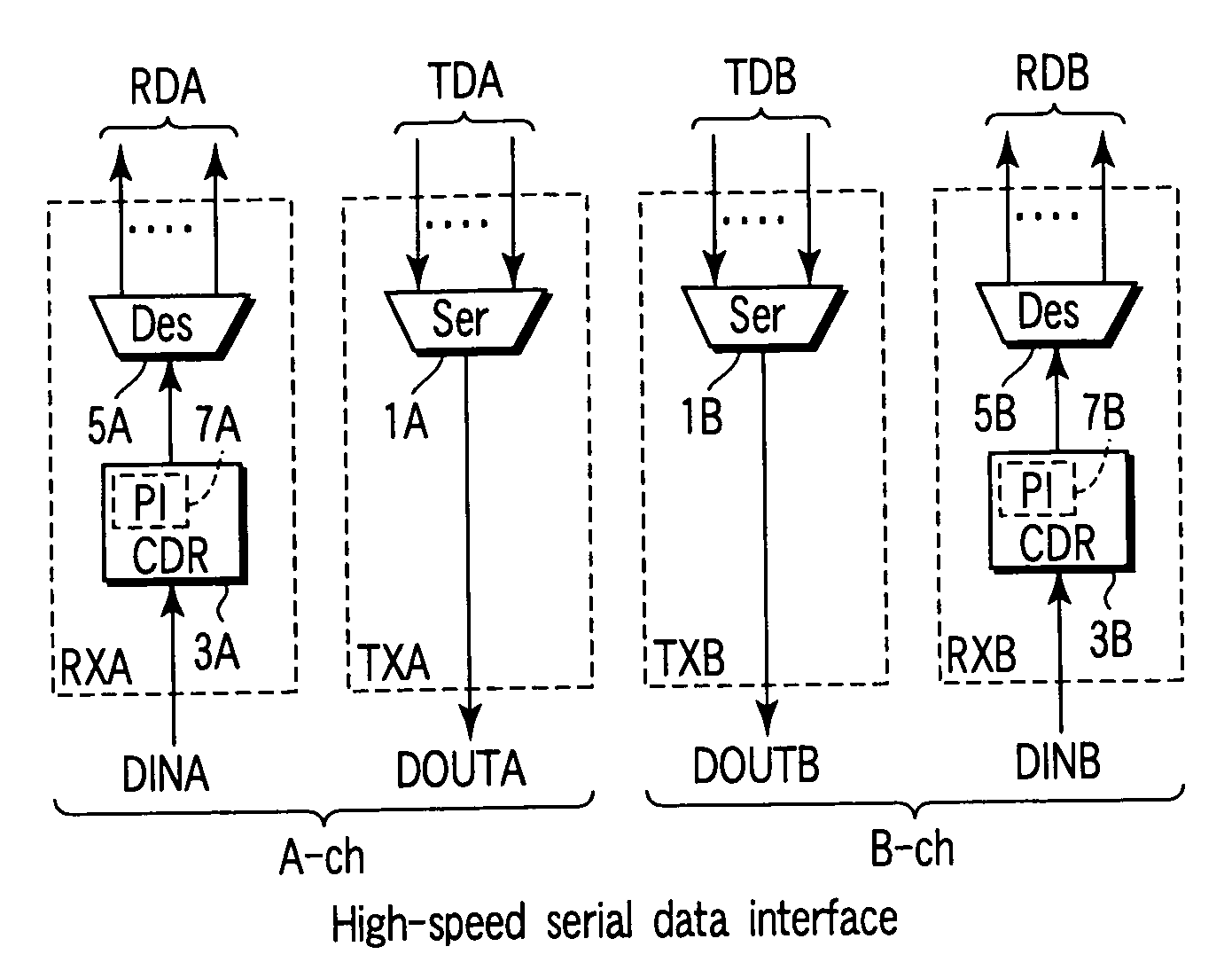
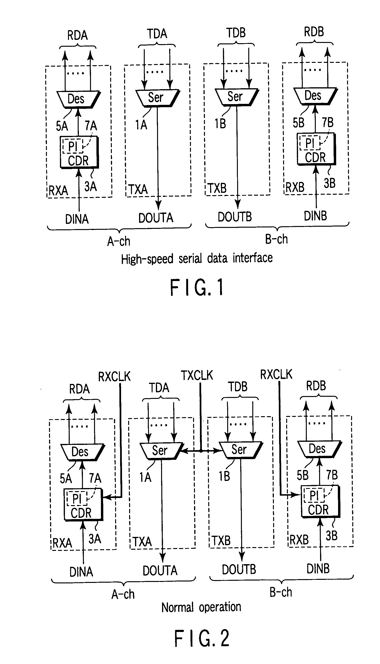
[0042]FIG. 1 is a block diagram showing the arrangement of a semiconductor integrated circuit device according to the first embodiment of the present invention. FIG. 2 is a block diagram showing the state of normal operation.

[0043] As shown in FIG. 1, this semiconductor integrated circuit device has a high-speed serial data interface. An example of a semiconductor integrated circuit device having a high-speed serial data interface is a transceiver which transmits and receives data. The high-speed serial data interface of the transceiver according to this embodiment is a multi-channel interface having two channels or more. In this embodiment, the interface has a first channel A-ch and second channel B-ch. The first channel A-ch includes a first transmitter TXA and first receiver RXA. The second channel B-ch includes a second transmitter TXB and second receiver RXB.

[0044] The first transmitter TXA includes a first serializer (Ser) 1A, and the second transmi...

Example

[0060] (Second Embodiment)

[0061] The second embodiment is a more definite example of the semiconductor integrated circuit device of the first embodiment.

[0062] In the second embodiment as this more definite example, new functional blocks for performing tests are added to the first embodiment. Examples of the added functional blocks and their configurations are as follows.

[0063] (A) Test Control Pattern Generating Circuit (TestGen)

[0064] A TestGen circuit generates phase control information necessary for a PI to shift the phase of a clock. For example, on the basis of information supplied from the outside of a high-speed serial data interface, the TestGen circuit outputs phase control information for shifting the phase of a clock to a CDR circuit.

[0065] (B) Test Analyzing Circuit (TestAna)

[0066] A TestAna circuit compares the phase shift amount of transmitted serial data with that of received serial data to check whether a CDR circuit has a problem.

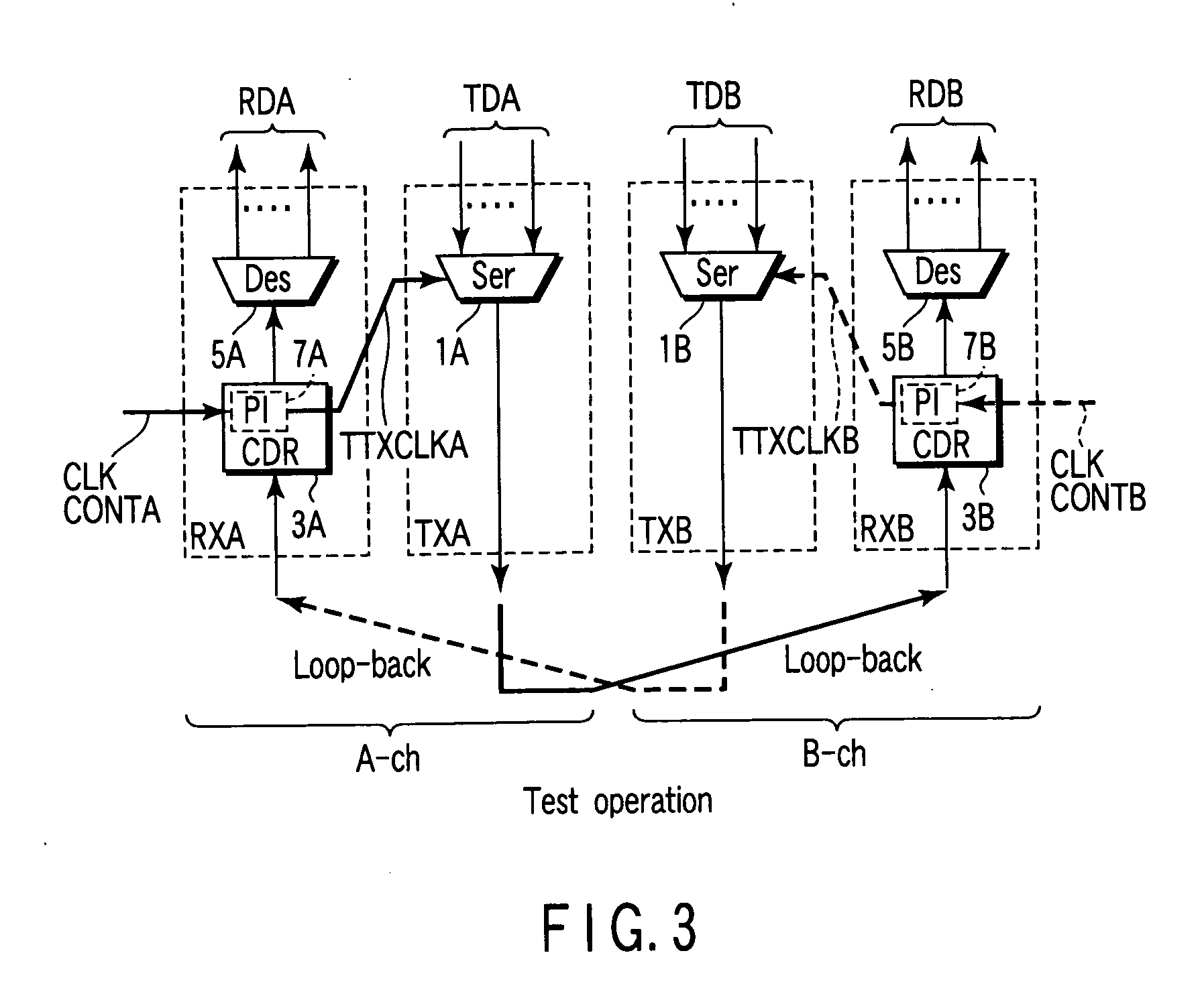
[0067] (C) Loop-Back Path (L...

Example

[0096] (Third Embodiment)

[0097]FIG. 10 is a block diagram showing the arrangement of a semiconductor integrated circuit device according to the third embodiment of the present invention.

[0098] As shown in FIG. 10, the third embodiment differs from the first and second embodiments in that receivers RX and transmitters TX are alternately arranged in the order of a first receiver RXA, first transmitter TXA, second receiver RXB, and second transmitter TXB.

[0099] Unlike in the first and second embodiments, the circuit pattern of the first receiver RXA and first transmitter TXA (to be referred to as a first channel A-ch hereinafter) and the circuit pattern of the second transmitter TXB and second receiver RXB (to be referred to as a second channel B-ch) are not arranged into, e.g., a mirror image pattern. However, it is possible to test the receivers without using an expensive high-speed tester, and improve the fault coverage.

[0100] In the third embodiment, unlike in the first and sec...


PUM


Abstract

A semiconductor integrated circuit device has first and second receivers and first and second transmitters. The first receiver has a first clock data recovery (CDR) circuit, and the second receiver has a second CDR circuit. Each of these first and second CDR circuits receives serial data, recovers a clock from the received serial data, and changes the phase of the generated clock. The first transmitter has a first serializer (SER), and the second transmitter has a second SER. The first SER converts parallel data into serial data synchronized with a transmit clock or the clock generated by the first CDR circuit. The second SER converts parallel data into serial data synchronized with a transmit clock or the clock generated by the second CDR circuit.

Description

CROSS-REFERENCE TO RELATED APPLICATIONS [0001] This application is based upon and claims the benefit of priority from the prior Japanese Patent Application No. 2003-308947, filed Sep. 1, 2003, the entire contents of which are incorporated herein by reference. BACKGROUND OF THE INVENTION [0002] 1. Field of the Invention [0003] The present invention relates to a semiconductor integrated circuit device and a method of testing the same and, more particularly, to a semiconductor integrated circuit device having a high-speed serial data interface and a method of testing the same. [0004] 2. Description of the Related Art [0005] A high-speed serial data interface has a serial data transmitter TX and serial data receiver RX. [0006] To test the transmitter TX of this high-speed serial data interface, it is only necessary to output data at low speed and check the pattern of the output data. [0007] In contrast, to test the receiver RX, data must be input to the receiver RX at high speed. Unfort...

Claims


Application Information

Patent Timeline
IPC IPC(8): H01L21/822G01R31/28H01L27/04H04B1/38
CPCG01R31/31716H03L7/0807H04L7/033H04L7/0025H04L7/0083H04L1/243
Inventor YOSHIOKA, SHINICHI
Owner KK TOSHIBA
Why Eureka
Try Eureka