Light emitting polymer devices with improved efficiency and lifetime

a technology of light-emitting polymer and efficiency, applied in the field of organic light-emitting diodes, can solve the problems of reducing device efficiency, reducing device lifetime, and reducing device efficiency

Inactive Publication Date: 2005-03-03
OSRAM OPTO SEMICONDUCTORS GMBH
View PDF13 Cites 39 Cited by
  • Summary
  • Abstract
  • Description
  • Claims
  • Application Information

AI Technical Summary

Problems solved by technology

In addition, there is a large energy barrier for hole injection at the interface between the HTL and the emissive layer that further suppresses the injection of holes into the emissive layer.
This often results in the emissive layer being hole deficient and this hole deficiency results in reduced device efficiency.
The hole deficiency also results in the recombination of electrons and holes that generate light to be localized in the region of the emissive layer that is very close to the HTL / emissive layer interface and the electrons that fail to recombine in this region leak into the HTL resulting in degradation of this layer and thus decreasing the lifetime of the device.
This imbalance between the number of electrons and holes in the emissive layer results in reduced device efficiency.
The injection of electrons into the HTL can degrade the HTL thus decreasing the device lifetime.

Method used


Image

  • Light emitting polymer devices with improved efficiency and lifetime
  • Light emitting polymer devices with improved efficiency and lifetime
  • Light emitting polymer devices with improved efficiency and lifetime

Examples


first embodiment

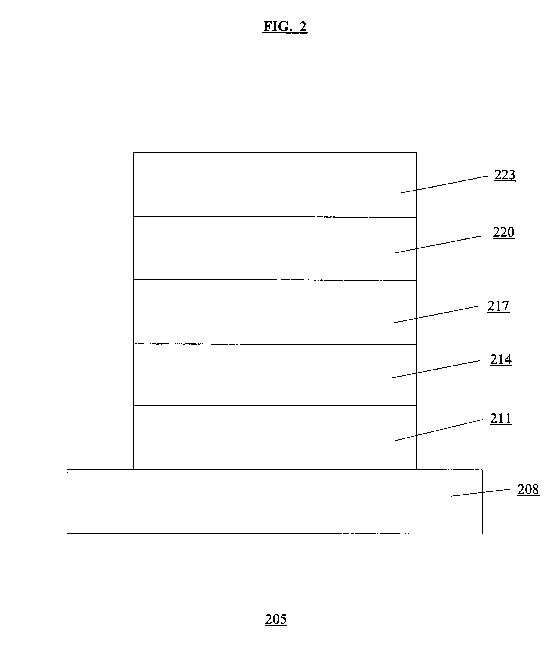
[0017]FIG. 2 shows a cross-sectional view of an OLED device 205 according to the present invention. The OLED device 205 can be, for example, a pixel within an OLED display, or an element within an OLED light source used for general purpose lighting. In FIG. 2, an anode 211 is on a substrate 208. As used within the specification and the claims, the term “on” includes when there is direct physical contact between the two parts and when there is indirect contact between the two parts because they are separated by one or more intervening parts. A first hole injection / transport layer 214 is on the anode 211. A second hole injection / transport layer 217 is on the first hole injection / transport layer 214. An emissive layer 220 is on the second hole injection / transport layer 217. A cathode 223 is on the emissive layer 220. The OLED device 205 may include other layers such as, for example, insulating layers between the anode 211 and the first hole injection / transport layer 214, and / or between...

second embodiment

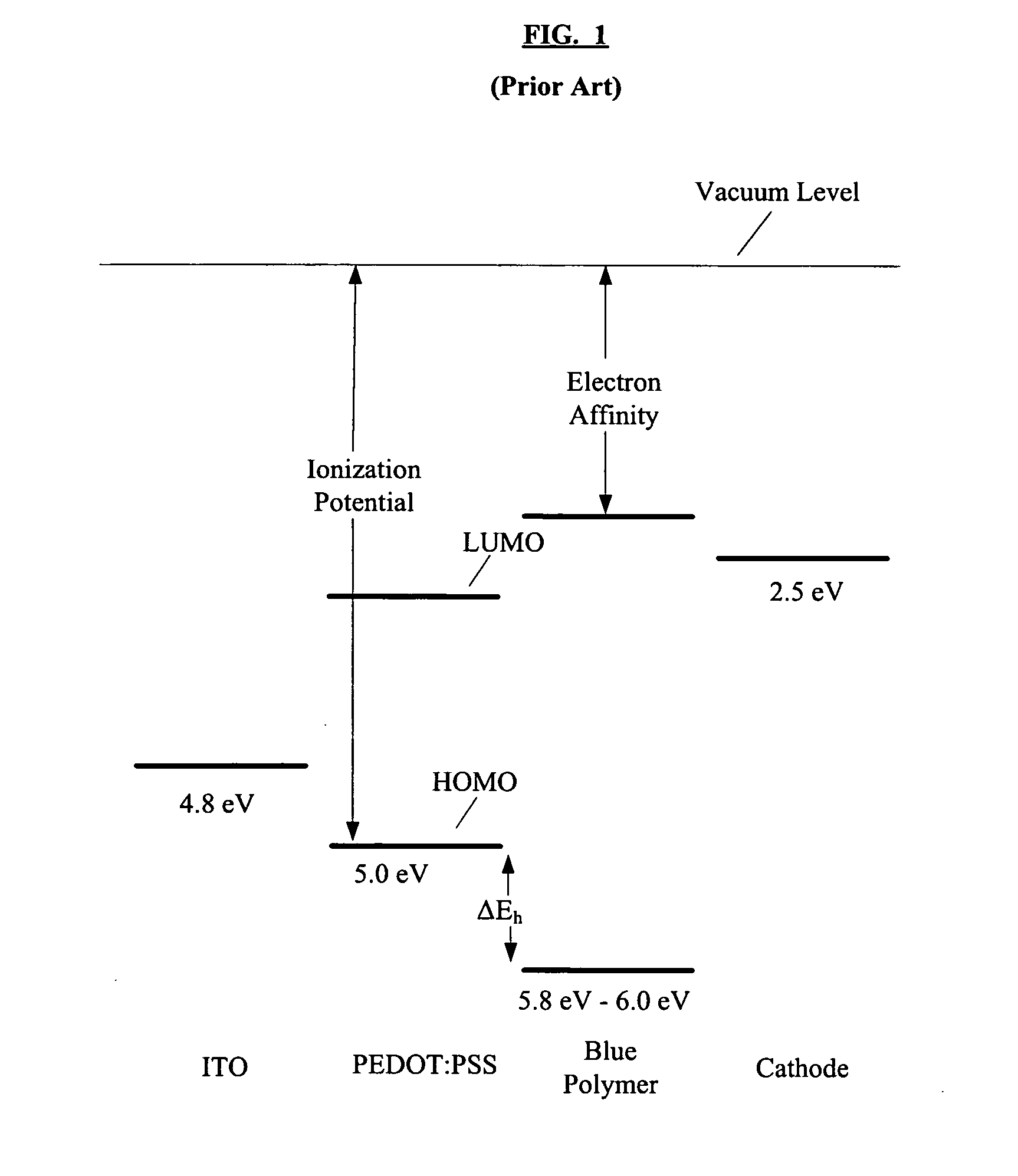
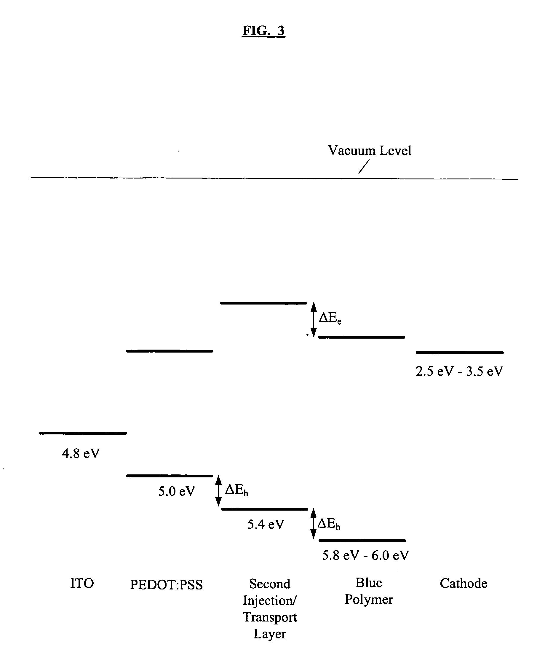
[0062] The first hole injection / transport layer may be comprised of materials such as PEDOT:PSS which contain many impurities. These impurities can contribute to decreased device performance such as, for example, shorter device lifetime. Also, the first hole injection / transport layer is a semiconductive material that increases the resistance of the device thus increasing the voltage needed to drive the device. Typically, as the operating voltage is increased, the device lifetime decreases. Therefore, in order to improve device performance and decrease the operating voltage, the first hole injection / transport layer can be eliminated. FIG. 5 shows a cross-sectional view of an OLED device 405 according to the present invention. In this embodiment, by including the second hole injection / transport layer within the device, the first hole injection / transport layer can be eliminated. In FIG. 5, an anode 411 is on a substrate 408. An injection / transport layer 417 is on the anode 411. An emis...


PUM

PropertyMeasurementUnit
thicknessaaaaaaaaaa
thicknessaaaaaaaaaa
HOMO energyaaaaaaaaaa

Abstract

In one embodiment of an OLED device, a hole injection/transport layer is added to the device structure in order to increase the number of holes injected into the emissive layer and reduce the number of electrons injected into the added hole injection/transport layer. In a first configuration of the added hole injection/transport layer, the added hole injection/transport layer is comprised of a non-doped hole transporting material that has an IP range between the highest IP value of the adjacent layer on the anode-end and the lowest IP value of the adjacent layer on the “emissive layer”-end. Optionally, in addition, nearly all electron affinities of the added hole injection/transport layer are less than the lowest electron affinity of the adjacent layer on the “emissive layer”-end. In a second configuration of the added hole injection/transport layer, this layer is formed by doping the hole transport material. The dopant is able to abstract electrons from the hole transporting material. By doping the hole transport material, the IP range of the hole transporting material is broadened. In addition or alternatively, the doping produces more HOMO energy states thus allowing more holes to occupy these intermediate states at any one time.

Description

CROSS-REFERENCE TO RELATED APPLICATIONS [0001] This application claims benefit of U.S. Provisional Patent Application having the Application Number: 60 / 499,095 filed on Aug. 28, 2003 and entitled “Light Emitting Polymer Devices with Improved Hole Injection Efficiency.”BACKGROUND OF THE INVENTION [0002] An organic light emitting diode (“OLED”) device typically includes, for example: (1) an anode on a substrate; (2) a hole transporting layer (“HTL”) on the anode; (3) an electron transporting and light emitting layer (“emissive layer”) on the HTL; and (4) a cathode on the emissive layer. When the device is forward biased, holes are injected from the anode into the HTL, and the electrons are injected from the cathode into the emissive layer. Both carriers are then transported towards the opposite electrode and allowed to recombine with each other in the device, the location of which is called the recombination zone. In this device configuration, the holes have to travel a longer distanc...

Claims


Application Information

Patent Timeline
Patent Type & Authority Applications(United States)
IPC IPC(8): H01L51/00H01L51/50H05B33/12
CPCH01L51/002H01L51/0036H01L51/0037H01L51/0038H01L51/0039H01L51/0043Y10T428/24942H01L51/0059H01L51/5048H01L51/5052H01L51/5088Y10T428/26H01L51/0051H10K71/30H10K85/114H10K85/115H10K85/1135H10K85/611H10K85/151H10K85/113H10K85/631H10K50/155H10K50/14H10K50/17
Inventor ANTONIADIS, HOMERALLEMAND, PIERRE-MARCSTEGAMAT, REZACHOONG, VI-EN
Owner OSRAM OPTO SEMICONDUCTORS GMBH
Why Eureka
Try Eureka