Basic cell, edge cell, wiring shape, wiring method, and shield wiring structure

a shielding and wire technology, applied in the field of shield wiring technique, can solve the problems of no free space left, man-hour wiring, etc., and achieve the effects of increasing processing difficulty, low regularity, and double the processing time required

Active Publication Date: 2005-03-03
PANASONIC SEMICON SOLUTIONS CO LTD
View PDF8 Cites 3 Cited by
  • Summary
  • Abstract
  • Description
  • Claims
  • Application Information

AI Technical Summary

Benefits of technology

[0024] According to the present invention, a plurality of wiring patterns each having a small area are prepared, and selection and arrangement of the wiring patterns are randomly performed, whereby shielding wires of low regularity, which is different from a simple array configuration, can be generated.
[0025] In a conventional shielding line, a route adjoins itself at a turn-around portion of a shield route. Thus, in the case where circuit analysis is committed with a probe against a circuit line in a shielding line removed region where a shielding line is removed and a cut shielding line is connected to another route, a region including two or more routes of shielding lines can be analyzed within a unit of processing time required for connecting the cut shielding line to another route. On the other hand, according to the present invention, a basic cell including a plurality of routes that extend constantly in parallel to one another and an edge cell for turn-around connection in which no route adjoins itself are provided. Even if circuit analysis is committed with a probe against a circuit line in a shielding line removed region, such a structure of the present invention doubles the processing time required for analysis in a region including two or more routes of shielding lines. Accordingly, the processing difficulty increases.
[0026] Further, a plurality of edge cells having different relationships of connection between terminals are used, whereby a shielding line route having less regularity is formed although the wiring of the uppermost layer has a regular pattern. Thus, the difficulty level of circuit analysis increases.

Problems solved by technology

However, a region to be shielded extends over the entire chip area, and therefore, manual wiring is impossible in view of the man-hour.
Further, an automatic wiring tool cannot place wires all over a chip area such that no free space is left.

Method used


Image

  • Basic cell, edge cell, wiring shape, wiring method, and shield wiring structure
  • Basic cell, edge cell, wiring shape, wiring method, and shield wiring structure
  • Basic cell, edge cell, wiring shape, wiring method, and shield wiring structure

Examples


embodiment 1

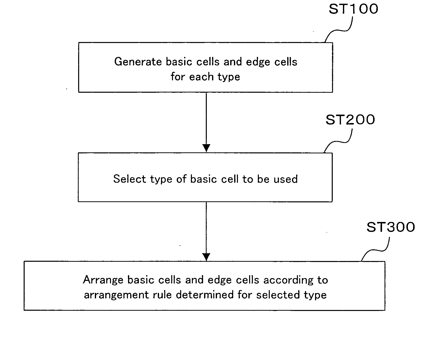
[0060]FIG. 1 shows a general procedure of a shielding line wiring method according to embodiment 1. A shielding line is provided in the uppermost wiring layer to hide a mask pattern, whereby reading of the mask pattern and circuit analysis with a probe on wires, which are performed for the purpose of copying and tampering of a semiconductor chip, are prevented. In embodiment 1, a plurality of wiring patterns (basic cells) each having a small area are prepared, and selection and arrangement of the wiring patterns are performed on a random basis. It should be noted that, as a matter of course, adjoining basic cells may have the same pattern. With this feature, shielding wires of low regularity, which is different from a simple array configuration, can be generated. Generation of such shield wiring is described below in detail.

[0061]

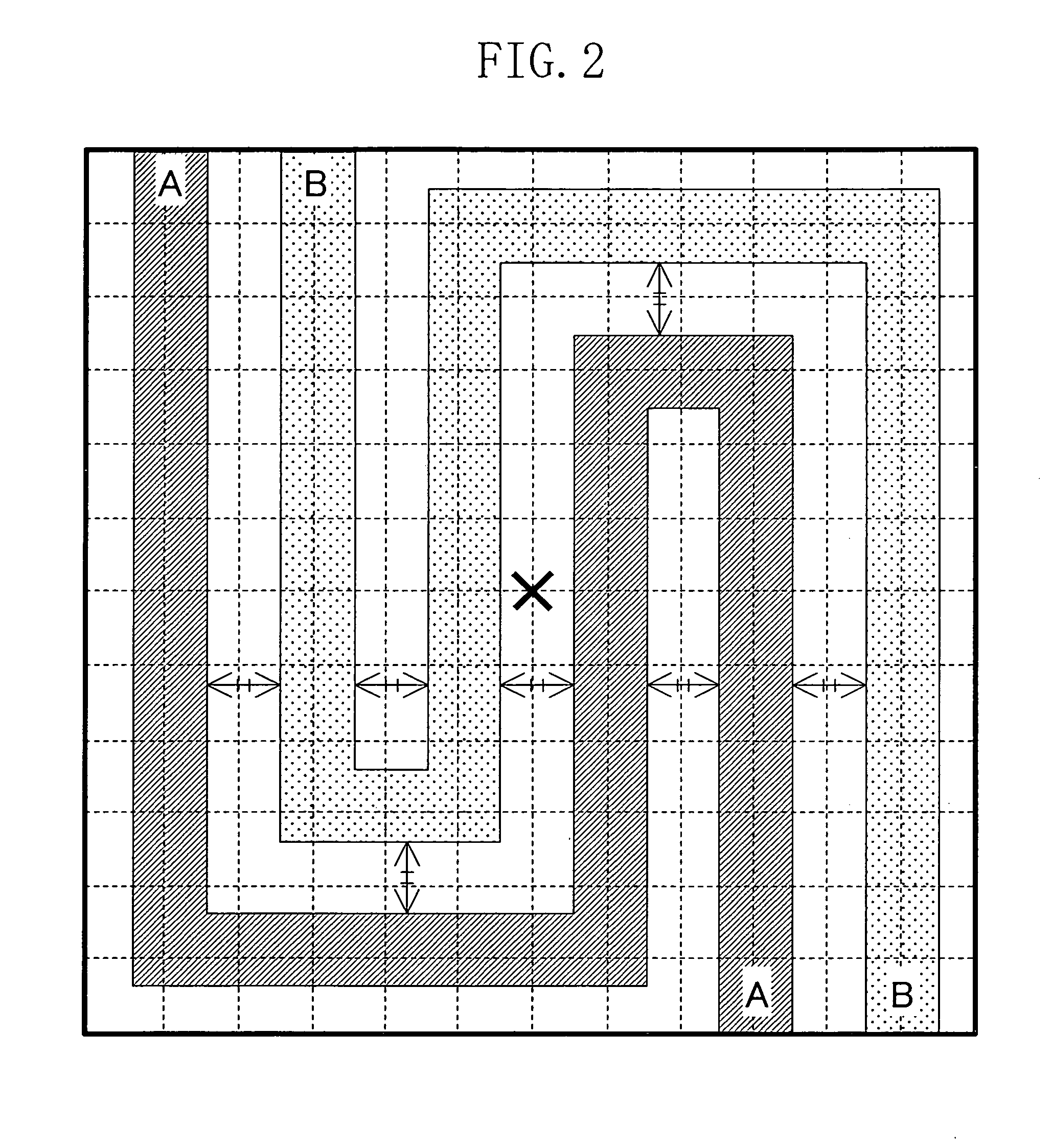
[0062] First, a design rule of a wiring pattern (basic cell) which is a basic unit of shield wiring is described. FIG. 2 shows an example of a basic cell,...

embodiment 2

[0124] The general procedure of the shielding line arrangement method of embodiment 2 is the same as that illustrated in FIG. 1. In embodiment 2, basic cells are arranged to form a plurality of constantly-parallel routes, and edge cells are arranged such that the same route is not adjacently provided (i.e., a route does not adjoin itself). Even if circuit analysis is committed with a probe against a circuit line in a shielding line removed region, the above structure of embodiment 2 doubles the processing time required for analysis in a region including two or more routes of shielding lines. Accordingly, the processing difficulty increases. This feature is specifically described below.

[0125]

[0126] First, a design rule of a basic cell which is a basic unit of the shielding line is described. Herein, the following design rule is provided for obtaining uniform wiring density: [0127] External boundary of a basic cell is rectangular; [0128] In the uppermost wiring layer, wires extend st...

embodiment 3

[0146] The structure of a basic cell according to embodiment 3 is shown in FIG. 30. In this basic cell, a 45°-route of the common 45°-wiring arrangement type basic cell illustrated in embodiments 1 and 2 is realized by a stepped route of 90°, whereby the difficulty level of treatment and processing of edge portions for 45° is lowered. In this basic cell, a stepped portion appears to be smooth like a 45°-wire. Further, due to the stepped shape, the exposed area of the underlying layer is small as compared with a common 45°-route. Although in FIG. 30 the entirety of the 45°-routes is realized by stepped 90°-routes, only a part of the 45°-routes may be realized by a stepped 90°-route. The basic cells illustrated in FIG. 30 are placed all over the shield region as in embodiments I and 2, whereby shielding lines are realized.


PUM


Abstract

A basic cell of the present invention comprises a plurality of wires which constitute a wiring route of 90°, one ends of the wires being on one of opposite sides, and the other ends of the wires being on the other one of the opposite sides, wherein: each of the one ends of the wires is point-symmetric to any of the other ends of the wires with respect to the center of the area of the basic cell; and routes of the plurality of wires do not cross one another.

Description

CROSS-REFERENCE TO RELATED APPLICATIONS [0001] This application claims priority under 35 U.S.C. §119(a) on Japanese Patent Application No. 2003-305392 filed on Aug. 28, 2003 and Japanese Patent Application No. 2004-183810 filed on Jun. 22, 2004, the entire contents of which are hereby incorporated by reference. BACKGROUND OF THE INVENTION [0002] 1. Field of the Invention [0003] The present invention relates to a shield wiring technique which increases the difficulty of physically analyzing a semiconductor chip to prevent fraudulent reading and tampering of security information. [0004] 2. Background Art [0005] In recent years, circuitry information and internal information of semiconductor devices have required a considerably high level of confidentiality and secrecy. Especially in the field of IC cards, the safety of semiconductor devices is an essential feature and, therefore, it is necessary to protect important information from fraudulent analysis and prevent tampering and copyin...

Claims


Application Information

Patent Timeline
Patent Type & Authority Applications(United States)
IPC IPC(8): G06F17/50H01L21/3205G06F21/00G06K19/073H01L21/28H01L21/288H01L21/3213H01L21/768H01L21/82H01L21/822H01L23/52H01L23/522H01L23/58H01L27/04H01L29/40H01L29/51
CPCG06F17/5077G06F21/75G06K19/07372H01L23/522H01L2924/0002H01L23/576H01L2924/00G06F30/394
Inventor MATSUNO, NORIAKITSUNODA, MASATOWADA, HIROFUMI
Owner PANASONIC SEMICON SOLUTIONS CO LTD
Why Eureka
Try Eureka