Semiconductor constructions, and methods of forming capacitor devices

Inactive Publication Date: 2005-03-10
ROUND ROCK RES LLC
View PDF40 Cites 127 Cited by
  • Summary
  • Abstract
  • Description
  • Claims
  • Application Information

AI Technical Summary

Benefits of technology

[0007] In one aspect, the invention encompasses methods of forming capacitor devices in which a construction comprising a first material is formed over a substrate, and a retaining structure is formed over at least a portion of the first material. Openings are formed to extend into the first material, and a first conductive layer is formed within the openings. The first conductive layer within the openings forms container structures having outer sidewalls along the first material. At least some of the first material is removed to ex

Problems solved by technology

Unfortunately, exposure of both the interior and exterior surfaces of a container having a high aspect ratio can render the container structurally weak, and subject to

Method used


Image

  • Semiconductor constructions, and methods of forming capacitor devices
  • Semiconductor constructions, and methods of forming capacitor devices
  • Semiconductor constructions, and methods of forming capacitor devices

Examples


Embodiment Construction

[0041] This disclosure of the invention is submitted in furtherance of the constitutional purposes of the U.S. Patent Laws “to promote the progress of science and useful arts” (Article 1, Section 8).

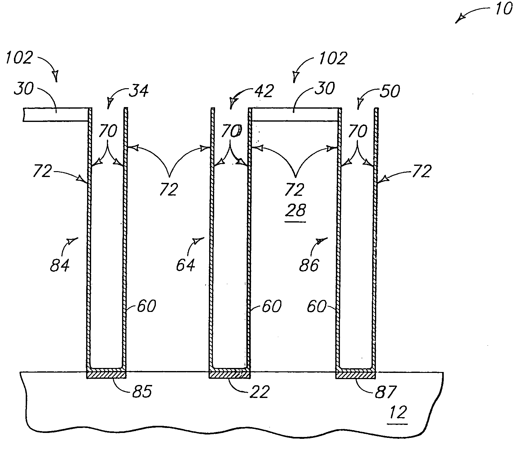
[0042] One aspect of the invention includes methodology for forming capacitor constructions in which a retaining structure, or lattice, is utilized to hold capacitor electrode structures (such as containers or pedestals) as outer sidewalls of the capacitor electrode structures are exposed with an etch. The retaining structure can thus alleviate, and preferably prevent, toppling and other structural defects occurring to the capacitor electrode structures as the outer surfaces of the structures are exposed. The capacitor electrode structures can be storage node structures.

[0043] A particular aspect of the invention includes methodology for forming container capacitor constructions in which a retaining structure, or lattice, is utilized to hold conductive containers as outer sidewalls of ...


PUM


Abstract

The invention includes semiconductor constructions, and also includes methods of forming pluralities of capacitor devices. An exemplary method of the invention includes forming conductive storage node material within openings in an insulative material to form conductive containers. A retaining structure lattice is formed in physical contact with at least some of the containers, and subsequently the insulative material is removed to expose outer surfaces of the containers. The retaining structure can alleviate toppling or other loss of structural integrity of the container structures. The electrically conductive containers correspond to first capacitor electrodes. After the outer sidewalls of the containers are exposed, dielectric material is formed within the containers and along the exposed outer sidewalls. Subsequently, a second capacitor electrode is formed over the dielectric material. The first and second capacitor electrodes, together with the dielectric material, form a plurality of capacitor devices.

Description

TECHNICAL FIELD [0001] The invention pertains to semiconductor constructions, and to methods of forming capacitor devices. BACKGROUND OF THE INVENTION [0002] Capacitor constructions continue to have increasing aspect ratios in higher generation integrated circuitry fabrication. For example, dynamic random access memory (DRAM) capacitors now have elevations of from 2 to 3 microns, with widths of about 0.1 micron. Further, it is a continuing goal to increase the density of semiconductor devices, with a corresponding goal to reduce the footprint associated with individual devices. As the packing density of capacitor devices becomes increasingly greater, the available surface area for capacitance decreases. [0003] A common capacitor construction is a so-called container device. One of the electrodes of such device is shaped as a container, and subsequently dielectric material and another capacitor electrode are formed within the container. Typically, only the interior surfaces of the co...

Claims


Application Information

Patent Timeline
IPC IPC(8): H01L21/02H01L21/3205H01L21/334H01L21/8242H01L27/02H01L27/108
CPCH01L27/0207H01L27/10817H01L29/66181H01L27/10894H01L28/91H01L27/10852H10B12/318H10B12/09H10B12/033H10B99/00H10B12/00
Inventor MANNING, H. MONTGOMERYGRAETTINGER, THOMAS M.PONTOH, MARSELA
Owner ROUND ROCK RES LLC
Why Eureka
Try Eureka