Full color organic electroluminescent device and method for fabricating the same

a full color, organic technology, applied in the direction of discharge tube luminescnet screen, discharge tube/lamp details, electric discharge lamps, etc., can solve the problems of difficult mass production of small molecular organic el devices, and reducing the emission efficiency of polymeric organic electroluminescent devices

Active Publication Date: 2005-03-17
SAMSUNG DISPLAY CO LTD
View PDF32 Cites 47 Cited by
  • Summary
  • Abstract
  • Description
  • Claims
  • Application Information

AI Technical Summary

Benefits of technology

[0018] Therefore, in order to solve the foregoing problems of the prior art, in one embodiment of the present invention, a full color organic electroluminescent device is provided that can be fabricated in fewer steps than are required for existing phosphorescence emitting devices. A method for fabricating the full color organic electroluminescent device is also provided.

Problems solved by technology

Mass production of a small molecular organic EL device is difficult since such a full color device is fabricated by depositing the respective layers using masks.
Such a polymeric organic electroluminescent device tends to have problems in its emission characteristics.
In particular, it generally has lower emission efficiency and reduced lifespan when fabricated using ink jet technology or laser induced thermal imaging.
Therefore, any process for forming an emitting layer is restricted since fine patterning should be performed for each of the red, green and blue colors to fabricate a full color organic electroluminescent device.
Prior art devices often have misalignment problems since the patterning process requires at least three deposition or transfer steps when forming the fine patterns of the red 100, green 200 and blue 300 on the pixel region.

Method used


Image

  • Full color organic electroluminescent device and method for fabricating the same
  • Full color organic electroluminescent device and method for fabricating the same
  • Full color organic electroluminescent device and method for fabricating the same

Examples


example 1

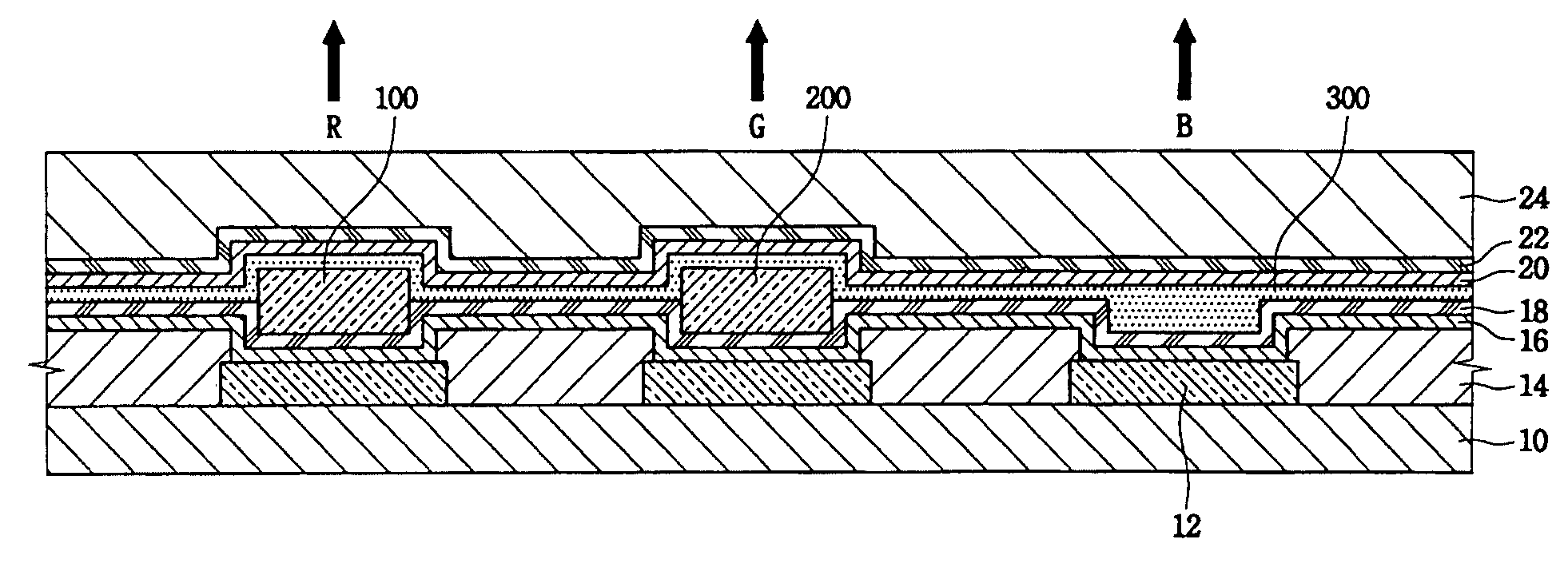
[0055] A hole injection layer having thickness of 30 nm formed of 4,4′,4″-tris(N-3-methylphenyl)-N-phenylamino)triphenylamine (MTDATA, Sensient Imaging Technologies GmbH) and a hole transport layer having thickness of 30 nm or less formed of N,N′-di(naphthalen-1-yl)-N,N′-diphenyl-benzidine (NPB) were formed on a patterned test cell. A red phosphorescence emitting layer was patterned and formed to a thickness of 35 nm from a host of CBP manufactured by UDC Corporation, doped with a dopant of R7 manufactured by UDC Corporation to a concentration of about 10%. A blue fluorescence emitting layer 10 nm thick was formed by doping a blue fluorescence emitting material of IDE 120 (manufactured by Idemitsu Corporation), with a DPVBi type dopant (Idemitsu Kosan) and applying the material to an upper part of the patterned red phosphorescence emitting layer and over the entire test cell. The red phosphorescence emitting layer was formed and patterned by laser induced thermal imaging. The test c...

example 2

[0056] A hole injection layer having a thickness of 30 nm formed of (4,4′,4″-tris(N-3-methylphenyl)-N-phenylamino)triphenylamine (MTDATA, Sensient Imaging Technologies GmbH) and a hole transport layer having a thickness of 30 nm or less formed of N,N′-di(naphthalen-1-yl)-N,N′-diphenyl-benzidine (NPB) were formed on a patterned test cell. A green phosphorescence emitting layer was patterned and formed with a thickness of 20 nm from a host of CBP manufactured by UDC Corporation, doped with a dopant of IrPPy manufactured by UDC Corporation to a concentration of about 5%. A blue fluorescence emitting layer 10 nm thick was formed by doping a blue fluorescence emitting material, IDE 120 (manufactured by Idemitsu Corporation), with DPVBi type dopant (Idemitsu Kosan) and applying the material to an upper part of the patterned green phosphorescence emitting layer and over the entire test cell. The green phosphorescence emitting layer was formed and patterned by laser induced thermal imaging....


PUM


Abstract

The present invention relates to a full color organic electroluminescent device and a method for fabricating the same and provides a full color organic electroluminescent device. The invention reduces misalignment errors caused by fine patterning of the emitting layer by reducing the steps of the fine patterning process. In particular, the blue emitting layer functions as a hole inhibition layer which results in superior color purity and improved stability for the color organic electroluminescent device. The use of such a blue emitting layer also reduces the manufacturing steps. The device comprises a substrate; a first electrode pattern formed on the substrate; a red emitting layer formed by patterning a red emitting material on a red pixel region of the first electrode pattern and a green emitting layer formed by patterning a green emitting material on a green pixel region of the first electrode pattern. A blue emitting layer is applied over the entire substrate, over the upper parts of the red and green emitting layers and a second electrode is formed on an upper part of the blue emitting layer.

Description

CROSS REFERENCE TO RELATED APPLICATIONS [0001] This application claims priority to and the benefit of Korean Patent Application No. 2003-63752, filed on Sep. 15, 2003, the disclosure of which is incorporated herein by reference in its entirety. BACKGROUND OF THE INVENTION [0002] 1. Field of the Invention [0003] The present invention relates to a full color organic electroluminescent device and a method for fabricating the full color organic electroluminescent device, more particularly, to a full color organic electroluminescent device with reduced pixel misalignment. [0004] 2. Description of Related Art [0005] Generally, an organic electroluminescent device comprises various layers including an anode and a cathode, a hole injection layer, a hole transport layer, an emitting layer, an electron transport layer and an electron injection layer. Organic electroluminescent devices are classified as polymeric organic EL (electroluminescent) devices and small molecular organic EL (electrolu...

Claims


Application Information

Patent Timeline
Patent Type & Authority Applications(United States)
IPC IPC(8): H05B33/12H01L27/32H01L51/00H01L51/30H01L51/50
CPCH01L27/3211H01L51/005H01L51/0059H01L51/5016H01L51/0081H01L51/0085H01L51/0062H10K59/35H10K85/60H10K85/649H10K85/631H10K85/324H10K85/342H10K50/11H10K2101/10H05B33/12
Inventor KIM, MU-HYUNCHIN, BYUNG-DOOSUH, MIN-CHULYANG, NAM-CHOULLEE, SEONG-TAEK
Owner SAMSUNG DISPLAY CO LTD
Why Eureka
Try Eureka