Direct application voltage variable material, devices employing same and methods of manufacturing such devices

a voltage variable material and direct application technology, applied in the field of circuit protection, can solve the problems of adding to the number of components required, and vvm devices consuming valuable board space,

Active Publication Date: 2005-03-17
LITTELFUSE INC
View PDF99 Cites 95 Cited by
  • Summary
  • Abstract
  • Description
  • Claims
  • Application Information

AI Technical Summary

Benefits of technology

[0027] It is therefore an advantage of the present invention to provide an intrinsically adhesive VVM.
[0028] Another advantage of the present invention is to provide a VVM that does not need to be housed in a separate device.
[0029] A further advantage of the present invention is to provide a VVM that is self-curing.
[0030] Yet another advantage of the present invention is to provide a VVM that adheres directly to a printed circuit board without the need for providing separate electrical pads on the substrate on which to mount the VVM.
[0031] Yet a further advantage of the present invention is to provide a VVM that adheres directly to a polymer or plastic.
[0032] Still another advantage of the present invention is to apply a VVM to a substrate directly, wherein the substrate is provided in an electrical device, such as a piece of equipment or a connector.

Problems solved by technology

Electrical overstress (“EOS”) transients produce high electric fields and usually high peak power that can render circuits or the highly sensitive electrical components in the circuits, temporarily or permanently non-functional.
This presents a variety of problems.
First, VVM devices add to the number of components that are required to be mounted to the PCB.
The VVM devices consume valuable board space and add to the potential for defects.
Second, adding components to an existing PCB can require a board redesign or other type of incorporation into a currently pending design.
If the application is already in production, it is likely that a considerable amount of time has been spent optimizing board space, which may or may not leave room to integrate a VVM device.
Third, many EOS transients occur outside of the PCB and are transmitted to the PCB through cables and wires.
For instance, networked computer and telephone systems are subject to a variety of transients caused by environmental and handling activities.

Method used


Image

  • Direct application voltage variable material, devices employing same and methods of manufacturing such devices
  • Direct application voltage variable material, devices employing same and methods of manufacturing such devices
  • Direct application voltage variable material, devices employing same and methods of manufacturing such devices

Examples


Embodiment Construction

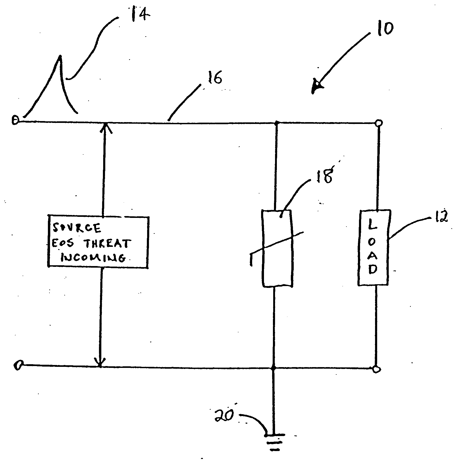
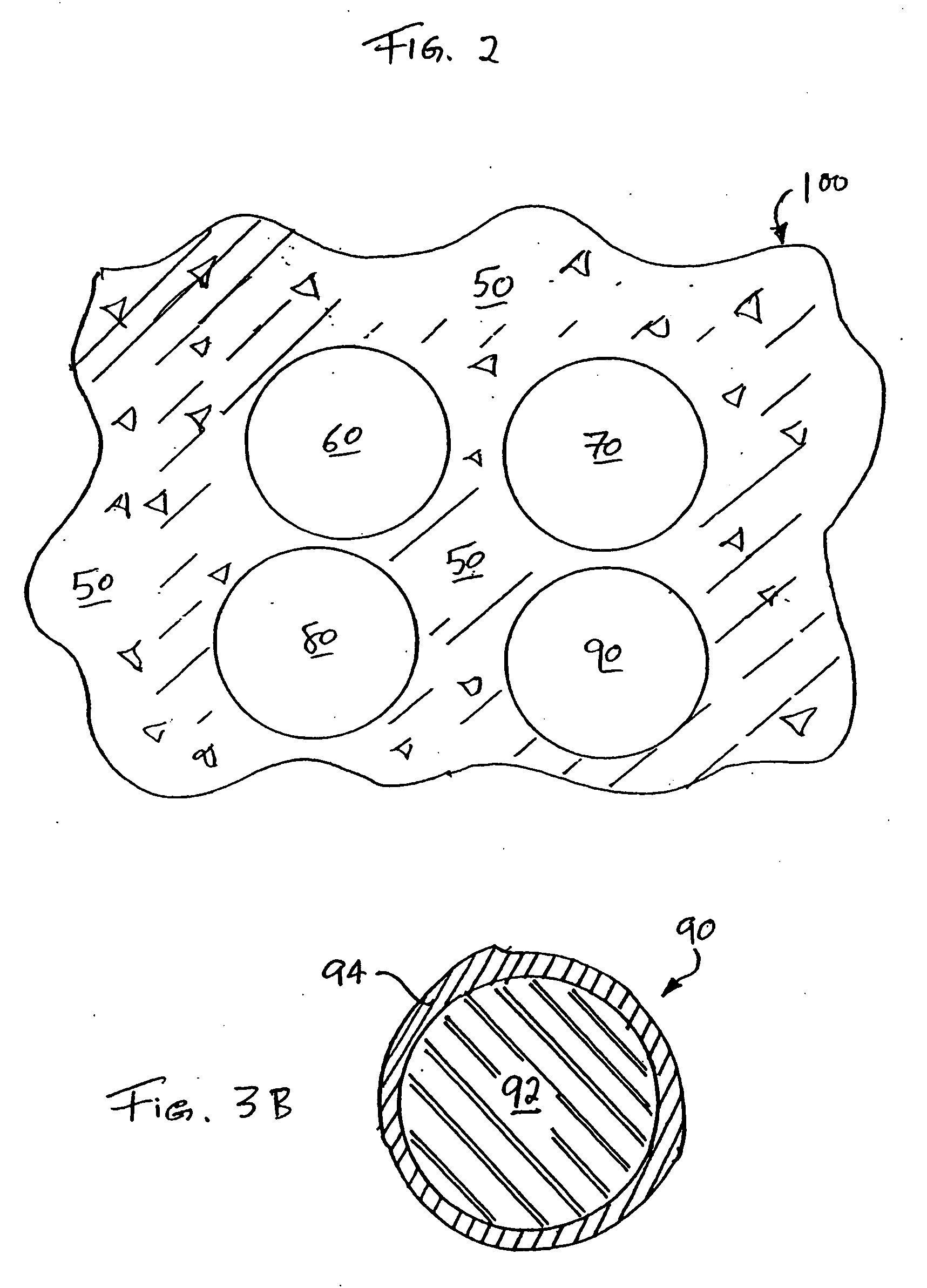
[0064] Referring now to FIG. 2, a voltage variable material (“VVM”) 100 of the present invention includes an insulative binder 50. The binder 50 secures one or more or all of certain different types of particles, such as insulating particles 60, semiconductive particles 70, doped semiconductive particles 80, conductive particles 90 and various combinations of these. The insulative binder 50 has intrinsically adhesive properties and self-adheres to surfaces, such as a conductive, metal surface or a non-conductive, insulative surface. The insulative binder 50 has a property of being self-curing, so that the VVM 100 can be applied to a circuit or application and be used thereafter without heating or otherwise curing the VVM 100 and the insulative binder 50. It should be appreciated, however, that the circuit or application employing the VVM 100 with the binder 50 may be heated or cured to accelerate the curing process.

Insulative Binder

[0065] The insulative binder 50 of the VVM 100 in...


PUM


Abstract

A voltage variable material (“VVM”) including an insulative binder that is formulated to intrinsically adhere to conductive and non-conductive surfaces is provided. The binder and thus the VVM is self-curable and applicable in a spreadable form that dries before use. The binder eliminates the need to place the VVM in a separate device or to provide separate printed circuit board pads on which to electrically connect the VVM. The binder and thus the VVM can be directly applied to many different types of substrates, such as a rigid FR-4 laminate, a polyimide, a polymer or a multilayer PCB via a process such as screen or stencil printing. In one embodiment, the VVM includes two types of conductive particles, one with a core and one without a core. The VVM can also have core-shell type semiconductive particles.

Description

PRIORITY CLAIM [0001] This application claims the benefit as a continuation-in-part of U.S. patent application Ser. No. 10 / 746,020, filed Dec. 23, 2003, entitled “Direct Application Voltage Variable Material, Components Thereof And Devices Employing Same,” which claims the benefit as a continuation-in-part of U.S. patent application Ser. No. 10 / 410,393, filed Apr. 8, 2003, entitled “Voltage Variable Material For Direct Application And Devices Employing Same,” which claims the benefit of U.S. Provisional Patent Application No. 60 / 370,975, filed Apr. 8, 2002, entitled “Voltage Variable Material For Direct Application And Devices Employing Same,” the entire contents of each which are hereby incorporated by reference and relied upon. CROSS-REFERENCE TO RELATED APPLICATIONS [0002] This application is related to the following commonly-owned co-pending patent applications: “Voltage Variable Substrate Material,” Ser. No. 09 / 976,964, Attorney Docket No. 0112690-098.BACKGROUND OF THE INVENTIO...

Claims


Application Information

Patent Timeline
Patent Type & Authority Applications(United States)
IPC IPC(8): H02H9/04H05K1/00H05K1/02H05K1/16
CPCH01C7/12H01G2/14H02H9/044H05K1/0257H05K1/0259H05K2201/09763H05K1/0393H05K1/167H05K3/28H05K2201/0738H05K1/0298
Inventor HARRIS, EDWIN JAMESVYAS, TUSHARPACHLA, TIMOTHYCOLBY, JAMES A.
Owner LITTELFUSE INC
Why Eureka
Try Eureka