Semiconductor memory device for improving access time in burst mode

a memory device and memory chip technology, applied in static storage, digital storage, instruments, etc., can solve the problems of giving the user discomfort, and unable to secure the time margin, so as to achieve the effect of improving the access time and avoiding increasing the chip area and power consumption

Active Publication Date: 2005-03-17
RENESAS ELECTRONICS CORP
View PDF3 Cites 8 Cited by
  • Summary
  • Abstract
  • Description
  • Claims
  • Application Information

AI Technical Summary

Benefits of technology

[0013] An object of the present invention is to solve the problems described above and to provide a semiconductor memory device in which the access time is improved in burst mode without increasing the chip area and power consumption.
[0019] Also, the parallel operation allows the data select circuit to have a margin of the select operation.

Problems solved by technology

Variations in the speed of reading the music information or the image information would cause discontinuous music or image reproduction and give the sense of discomfort to the user.
Therefore, no time margin can be secured for reading from the memory cell, thereby leading to the problem that it is difficult to output the data continuously.
Since the sense amplifiers and the latches occupy a large area of the chip, however, the disadvantage is encountered that the chip area is increased as compared with the ordinary semiconductor memory device.
Also, the provision of a sense amplifier for each bit line greatly increases the power consumption for reading the data.
In an application to a battery-driven portable information device, therefore, the operating time of the portable information device is undesirably shortened.

Method used


Image

  • Semiconductor memory device for improving access time in burst mode
  • Semiconductor memory device for improving access time in burst mode
  • Semiconductor memory device for improving access time in burst mode

Examples


second embodiment

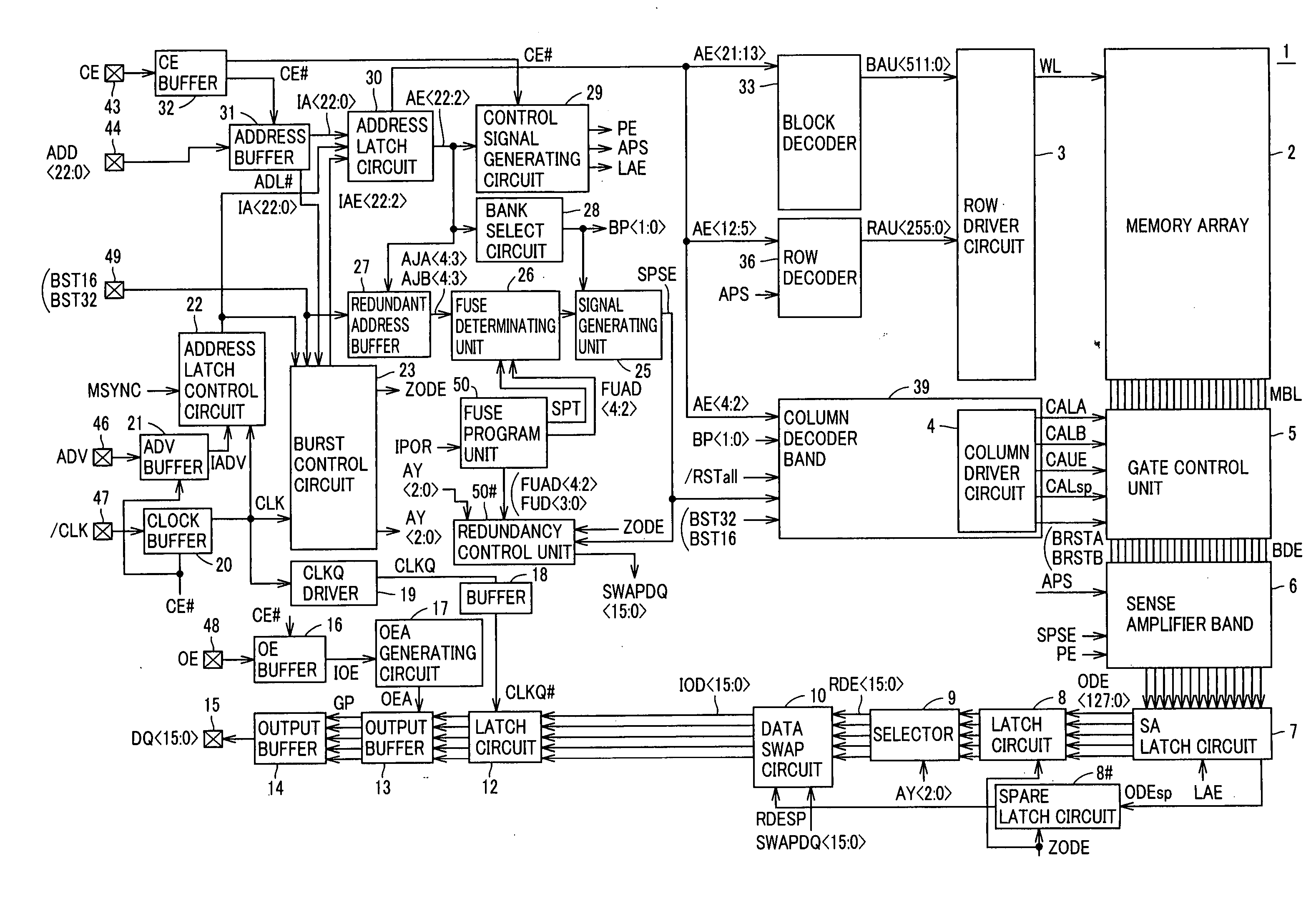
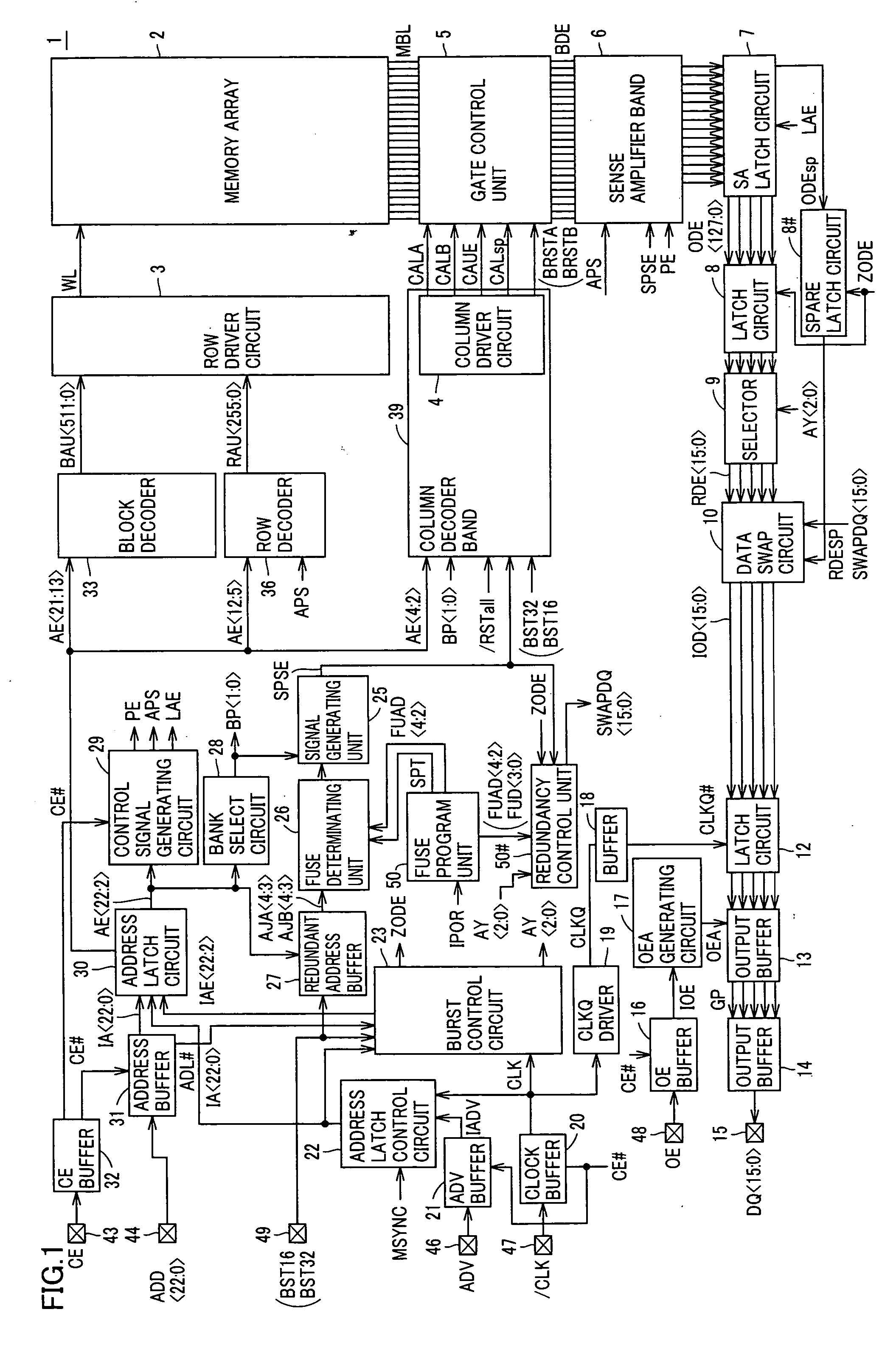
[0158] The second embodiment refers to a redundant configuration in the memory array described with reference to the first embodiment.

[0159] Referring to FIG. 16, the address conversion similar to the one employed for the column decoder CDCA0 is required for this redundant address buffer 27.

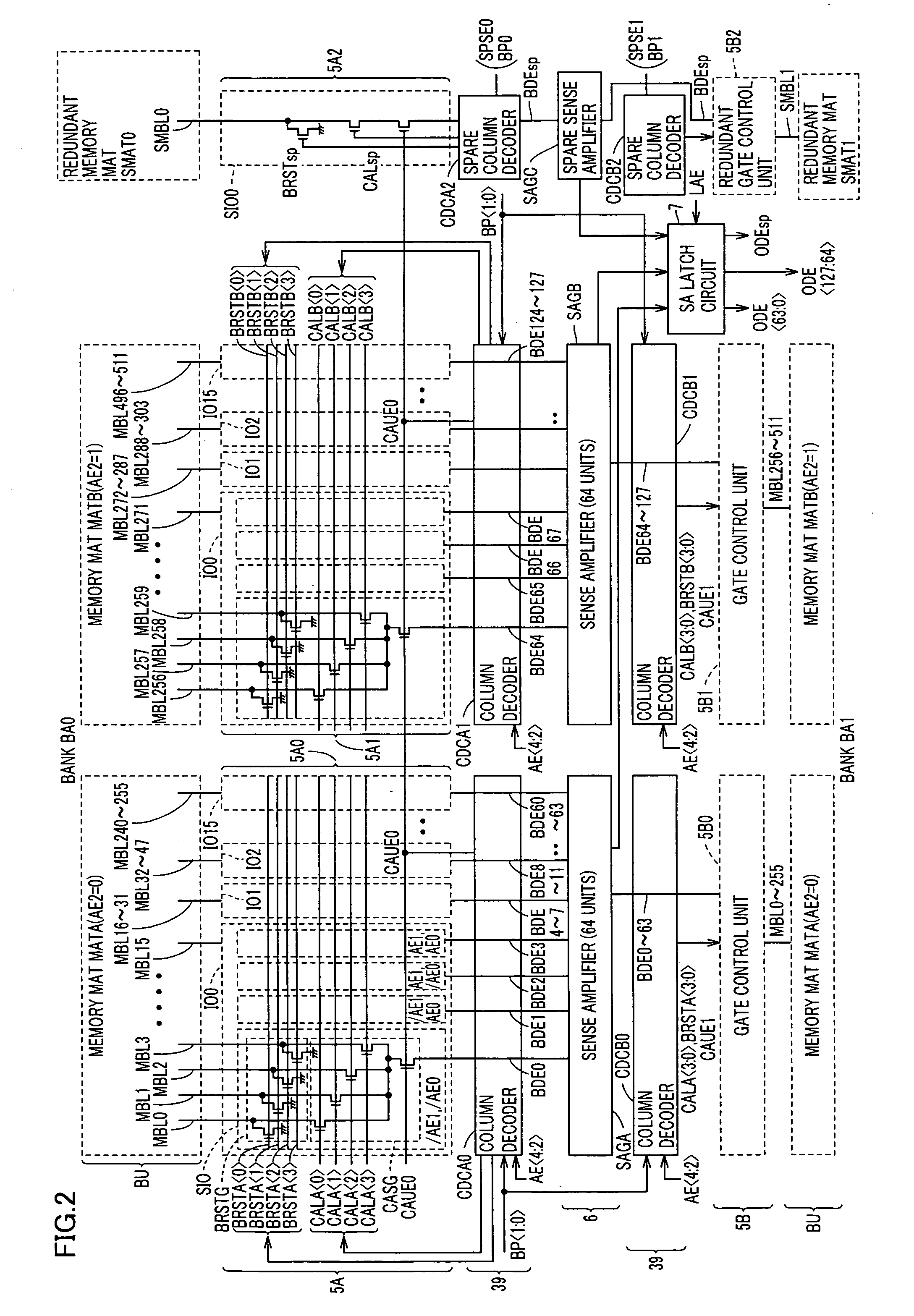
[0160] The address conversion for redundancy determination is carried out based on the input of internal address AE. Specifically, AND circuit AD10, exclusive OR circuits ER2, ER3 make up an address conversion circuit. The operation is similar to the one described above for column decoder CDCA0. In the case where internal address AE2 is “1”, the address is converted and internal address AJA is generated. In the case where internal address AE2 is “0”, on the other hand, AJB is generated. Specifically, internal addresses AJA and AJB for determination are generated for memory mat MATA with internal address AE2 of “0” and memory mat MATB with internal address AE2 of “1”, respectively.

[0161] Referr...

third embodiment

[0195] In the word line select operation in APS (Automatic Power Saving) mode, word line WL, once activated, is deactivated after the data of the sense amplifier is established a predetermined time later. Then, the same word line WL, if selected again in burst mode, is required to be reactivated, resulting in great current consumption for charge and discharge operation. According to the third embodiment, the operation of canceling the APS mode is carried out during the burst mode to reduce power consumption thereby to maintain the state in which word line WL is selected.

[0196] Referring to FIG. 26, memory device 1# according to the third embodiment is different in the provision of APSBST signal generating unit 11. The other points are the same as those described for memory device 1 and therefore not described in detail again.

[0197] APSBST signal generating unit 11 outputs control signal APSBST to row decoder 36 based on the input of control signal APS.

[0198] Referring to FIG. 27,...


PUM


Abstract

A semiconductor memory device is disclosed. A block unit is divided into memory mats based on an internal address. In the case where the internal address is “1”, data are read in ascending order in accordance with a start address from the memory mat, while the internal address is incremented by an address conversion circuit thereby to select a 4-word block including the words next selected from the memory mat. At the same time, the internal address is incremented based on the start address, so that the period for reading each word included in the lowest order of 4-word block can be secured. In the process, the address next to be input can be decoded.

Description

BACKGROUND OF THE INVENTION [0001] 1. Field of the Invention [0002] The present invention relates to a semiconductor memory device having a burst access mode capable of high-speed read operation. [0003] 2. Description of the Background Art [0004] In recent years, the progress of the process technique has improved the integration degree of a semiconductor memory device with an increased operating speed. Especially, the operating speed of the CPU (Central Processing Unit) has remarkably increased. In keeping with the operating speed of the CPU, therefore, the program data stored in the semiconductor memory device is required to be read at high speed. Demand is high, therefore, for an increased speed of the read operation of the semiconductor memory device. [0005] Specifically, the music information and the image information such as animation have come to be stored in a single semiconductor chip. The music information can now be reproduced through the speaker or the image information c...

Claims


Application Information

Patent Timeline
Patent Type & Authority Applications(United States)
IPC IPC(8): G11C17/00G11C7/00G11C7/10G11C8/00G11C8/04G11C16/26G11C16/32G11C17/12G11C17/18G11C29/00G11C29/04
CPCG11C7/103G11C16/26G11C29/846G11C29/789G11C16/32G11C7/06G11C7/12G11C8/04G11C16/24G11C29/787
Inventor YAMAUCHI, TADAAKIKUBO, TAKASHI
Owner RENESAS ELECTRONICS CORP
Why Eureka
Try Eureka