Process for making byte erasable devices having elements made with nanotubes

a technology of nanotubes and switching elements, which is applied in the field of manufacturing devices using transistors and nanotube switching elements, can solve the problems of long write cycles (ms), low relative speed in comparison to dram or sram, and relatively low cost of rom,

Inactive Publication Date: 2005-03-17
NANTERO
View PDF51 Cites 75 Cited by
  • Summary
  • Abstract
  • Description
  • Claims
  • Application Information

AI Technical Summary

Problems solved by technology

ROM is relatively low cost but cannot be rewritten.
EEPROM (or “Flash”) is inexpensive, and has low power consumption but has long write cycles (ms) and low relative speed in comparison to DRAM or SRAM.
Flash also has a finite number of read / write cycles leading to low long-term reliability.
SRAM does not need to be refreshed and is fast relative to DRAM, but has lower density and is more expensive relative to DRAM.
Both SRAM and DRAM are volatile, meaning that if power to the memory is interrupted the memory will lose the information stored in the memory cells.
Consequently, existing technologies are either non-volatile but are not randomly accessible and have low density, high cost, and limited ability to allow multiple writes with high reliability of the circuit's function, or they are volatile and complicate system design or have low density.
A different memory cell based upon magnetic tunnel junctions has also been examined but has not led to large-scale commercialized MRAM devices.
FRAM suffers from a large memory cell size, and it is difficult to manufacture as a large-scale integrated component.
While the nonvolatility condition is met, this technology appears to suffer from slow operations, difficulty of manufacture and poor reliability and has not reached a state of commercialization.
This form of memory requires highly specialized wire junctions and may not retain non-volatility owing to the inherent instability found in redox processes.
These techniques are now believed to be difficult to employ at commercial scales using modern technology.
Moreover, they may contain inherent limitations such as the length of the nanotubes that may be grown reliably using these techniques, and it may difficult to control the statistical variance of geometries of nanotube wires so grown.

Method used


Image

  • Process for making byte erasable devices having elements made with nanotubes
  • Process for making byte erasable devices having elements made with nanotubes
  • Process for making byte erasable devices having elements made with nanotubes

Examples


Embodiment Construction

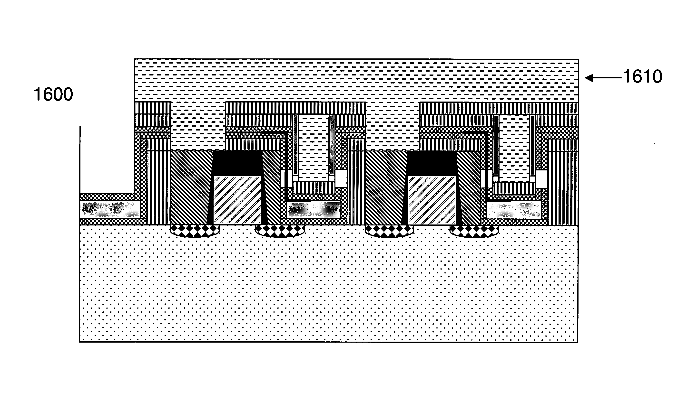
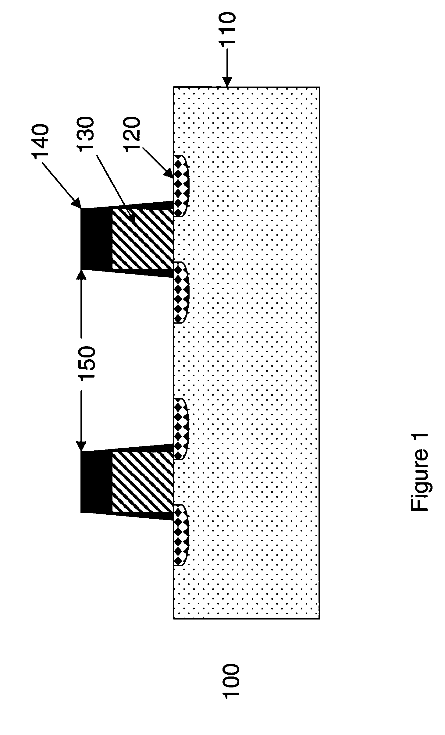
[0043] The device made by the present invention can be described by its cell size. For a bit selectable, Byte / Word erasable cell, 1T-cell, (a one transistor cell) the minimum cell size would be 8 F2, (F2 is a reference to the smallest feature size, squared.) Advantages of using this method include, that most likely no new tooling would be required to perform the methods in a fabrication plant. Nanotubes are dispensed by regular spin-coating and patterned using traditional lithography. Nanotube switching element requires controlled air gap and anchor to structures adjacent to the gap.

[0044] A typical nanotube device is composed of a nanofabric as described in U.S. patent application Ser. No. 09 / 915093, Electromechanical Memory Array Using Nanotube Ribbons and Method for Making Same, filed Jul. 25, 2001 (NAN-1); U.S. patent application Ser. No. 09 / 915173, Electromechanical Memory Having Cell Selection Circuitry Constructed with Nanotube Technology, filed Jul. 25, 2001 (NAN-2);

[0045]...


PUM


Abstract

A method of making byte erasable devices having elements made with nanotubes. Under one aspect of the invention, a device is made having nanotube memory elements. A structure is provided having a plurality of transistors, each with a drain and a source with a defined channel region therebetween, each transistor further including a gate over said channel. For a predefined set of transistors, a corresponding trench is formed between gates of adjacent transistors. For each trench, a defined pattern of nanotube fabric is provided over at least a horizontal portion of the structure and extending into the trench. An electrode is provided in each trench. Each defined pattern of nanotube fabric is suspended so that at least a portion is vertically suspended in spaced relation to the vertical walls of the trench and positioned so that the vertically suspended defined pattern of nanotube fabric is electromechanically deflectable into electrical communication with one of the drain and source of a transistor. An electrical communication path is provided electrically connecting each electrode so that all electrodes may electro-statically attract a corresponding defined pattern of nanotube fabric away from a transistor and toward the electrode.

Description

CROSS-REFERENCE TO RELATED APPLICATIONS [0001] This application claims priority under 35 USC § 119(e) to the following application, which is hereby incorporated by reference in its entirety: [0002]“Byte Erasable Process”, U.S. Provisional Pat. Apl. Ser. No. 60 / 464625, filed on Apr. 22, 2003. [0003] The following applications are related and are hereby incorporated by reference in their entirety: [0004]“Electro-Mechanical Switches and Memory Cells Using Horizontally-Disposed Nanofabric Articles and Methods of Making the Same”, U.S. Provisional Pat. Apl. Ser. No. 60 / 446783), filed on Feb. 12, 2003; [0005]“Electro-Mechanical Switches and Memory Cells Using Vertically-Disposed Nanofabric Articles and Methods of Making the Same”, U.S. Provisional Pat. Apl. Ser. No. 60 / 446786), filed on Feb. 12, 2003; [0006]“Combined Three Terminal and Four Terminal Nanotube / FET Structures”, U.S. Provisional Pat. Apl. Ser. No. 60 / 512602, filed on Oct. 16, 2003; [0007] NRAM Bit Selectable Two-Device Nanotu...

Claims


Application Information

Patent Timeline
Patent Type & Authority Applications(United States)
IPC IPC(8): G11C13/02G11C23/00H01L51/00
CPCB82Y10/00G11C13/025Y10S977/943H01L51/0048G11C23/00H10K85/221
Inventor RUECKES, THOMASJAIPRAKASH, VENKATACHALAM C.BERTIN, CLAUDE L.
Owner NANTERO
Why Eureka
Try Eureka