

Method of forming a resist pattern and fabricating tapered features
a technology of resist pattern and tapered features, which is applied in the field of fabrication of microelectronic devices, can solve the problems of difficult control of taper angle and incomplete formation of holes, and achieve the effect of accurate control and high reliability
- Summary
- Abstract
- Description
- Claims
- Application Information
AI Technical Summary
Benefits of technology
Problems solved by technology
Method used
Image

Examples
first embodiment
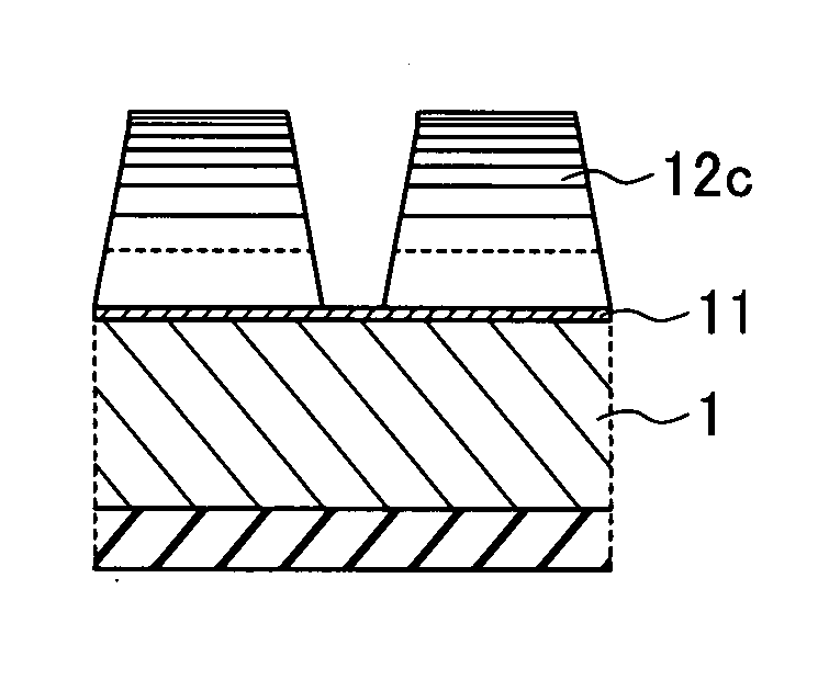
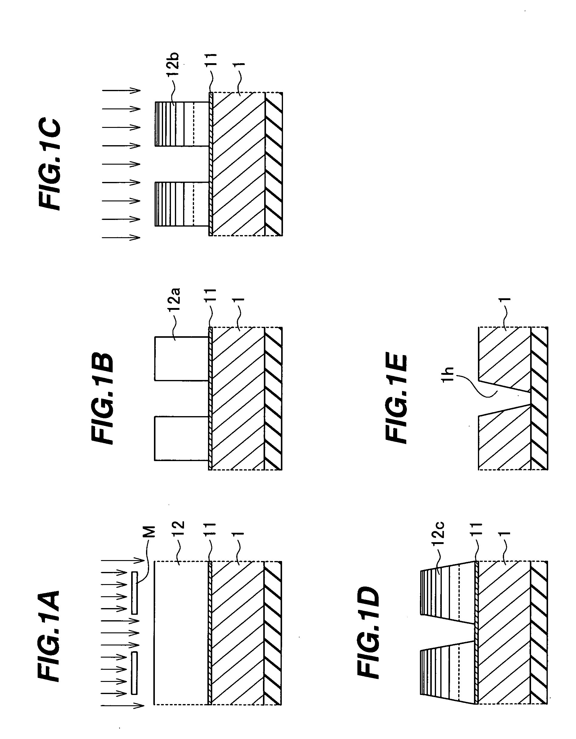
[0016] (Step 1) As shown in FIG. 1A, the surface of a semiconductor substrate such as a silicon (Si) wafer substrate 1 is given an antireflection coating 11 approximately 110 nm thick, then coated with a photoresist 12 having a glass transition temperature that increases under irradiation by an electron beam. An example of a suitable photoresist is the SEPR411 chemically amplified positive photoresist made by Shin-Etsu Chemical Co., Ltd. The photoresist coating is approximately 1000 nm thick. The substrate and its coatings are baked at a temperature of about 100 degrees Celsius; then a krypton fluoride (KrF) excimer laser exposure system (numerical aperture=0.60, σ=0.75) is used to expose the photoresist 12 to approximately 95 mJ / cm2 of ultraviolet light through a mask M having a desired circuit design pattern, including hole patterns 0.28 μm in diameter.
[0017] (Step 2) After the exposure, the photoresist 12 is developed in a 2.38 percent (%) tetramethyl ammonium hydroxide (TMAH) d...
second embodiment
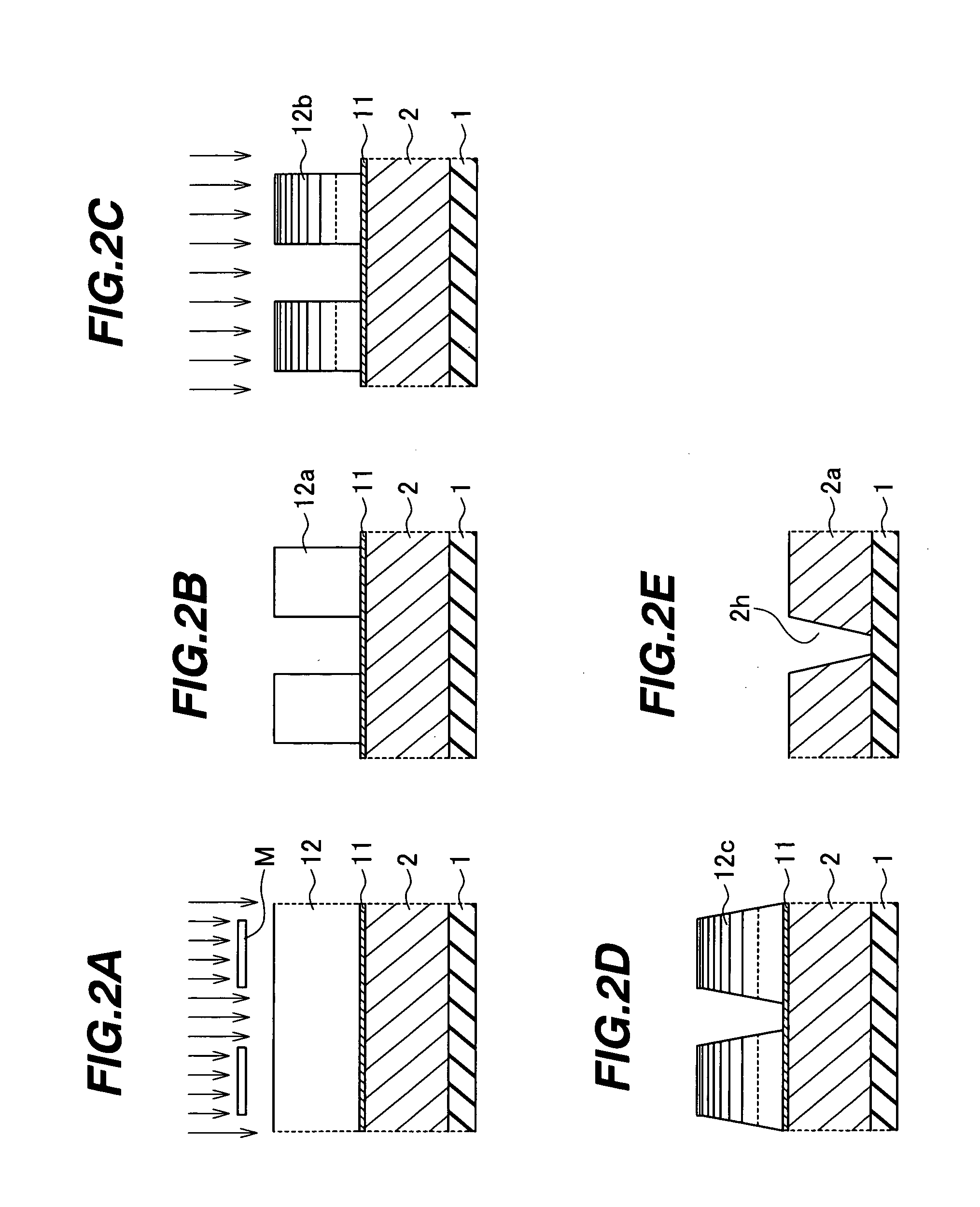
[0022] (Step 1) A silicon substrate 1 is processed to form isolation regions and gate electrodes (not shown); then an interlayer dielectric film 2 such as a silicon oxide film (nondoped silicate glass, NSG) approximately 1000 nm thick is formed on the surface of the silicon substrate 1. The word ‘substrate’ will be used below to refer to both the silicon substrate 1 and the interlayer dielectric film 2. The substrate surface is coated with an antireflection coating 11 with a thickness of approximately 110 nm; then a photoresist 12 having a glass transition temperature that increases under irradiation by an electron beam is coated onto the antireflection coating 11 to a thickness of approximately 1000 nm, and baked at a temperature of about 100 degrees Celsius.
[0023] Next, as shown in FIG. 2A, the photoresist 12 is exposed to ultraviolet light at approximately 95 mJ / cm2 by a KrF excimer laser exposure system (numerical aperture=0.60, σ=0.75), through a mask M having a desired circui...
PUM
| Property | Measurement | Unit |
|---|---|---|
| diameter | aaaaa | aaaaa |
| diameter | aaaaa | aaaaa |
| thick | aaaaa | aaaaa |
Abstract
Description
Claims
Application Information