

Power semiconductor element capable of improving short circuit withstand capability while maintaining low on-voltage and method of fabricating the same
- Summary
- Abstract
- Description
- Claims
- Application Information
AI Technical Summary
Benefits of technology
Problems solved by technology
Method used
Image

Examples
first embodiment
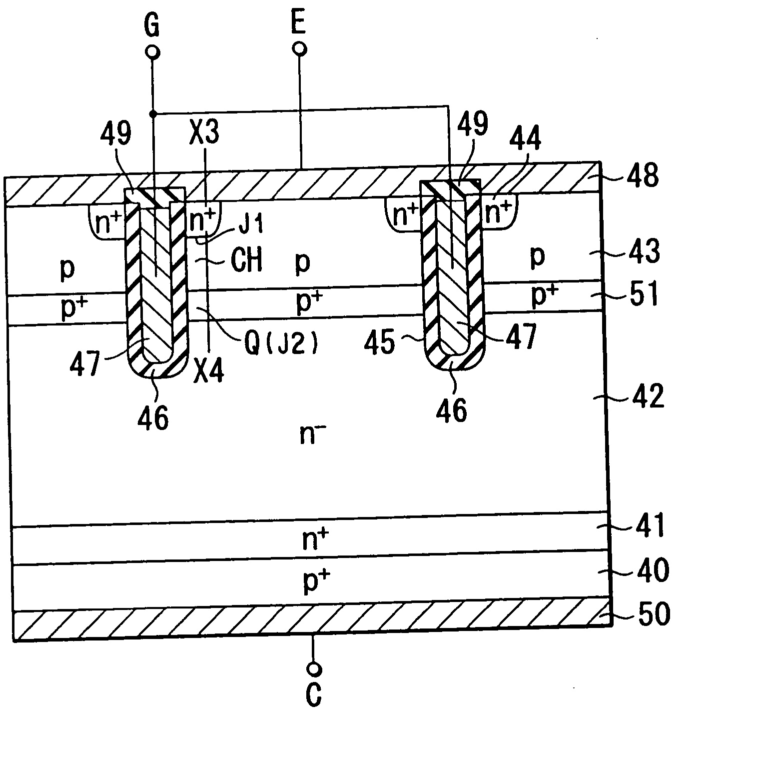
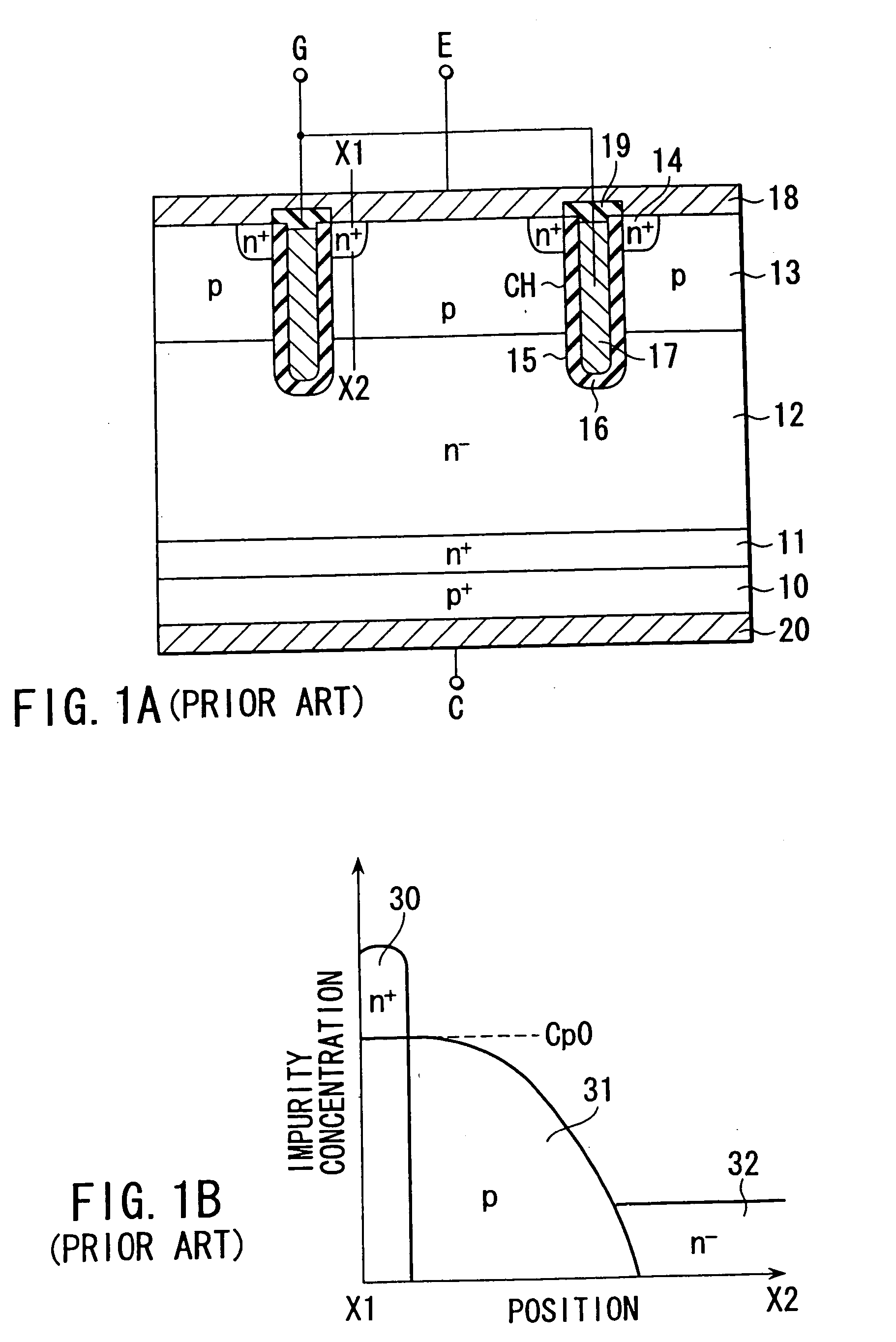
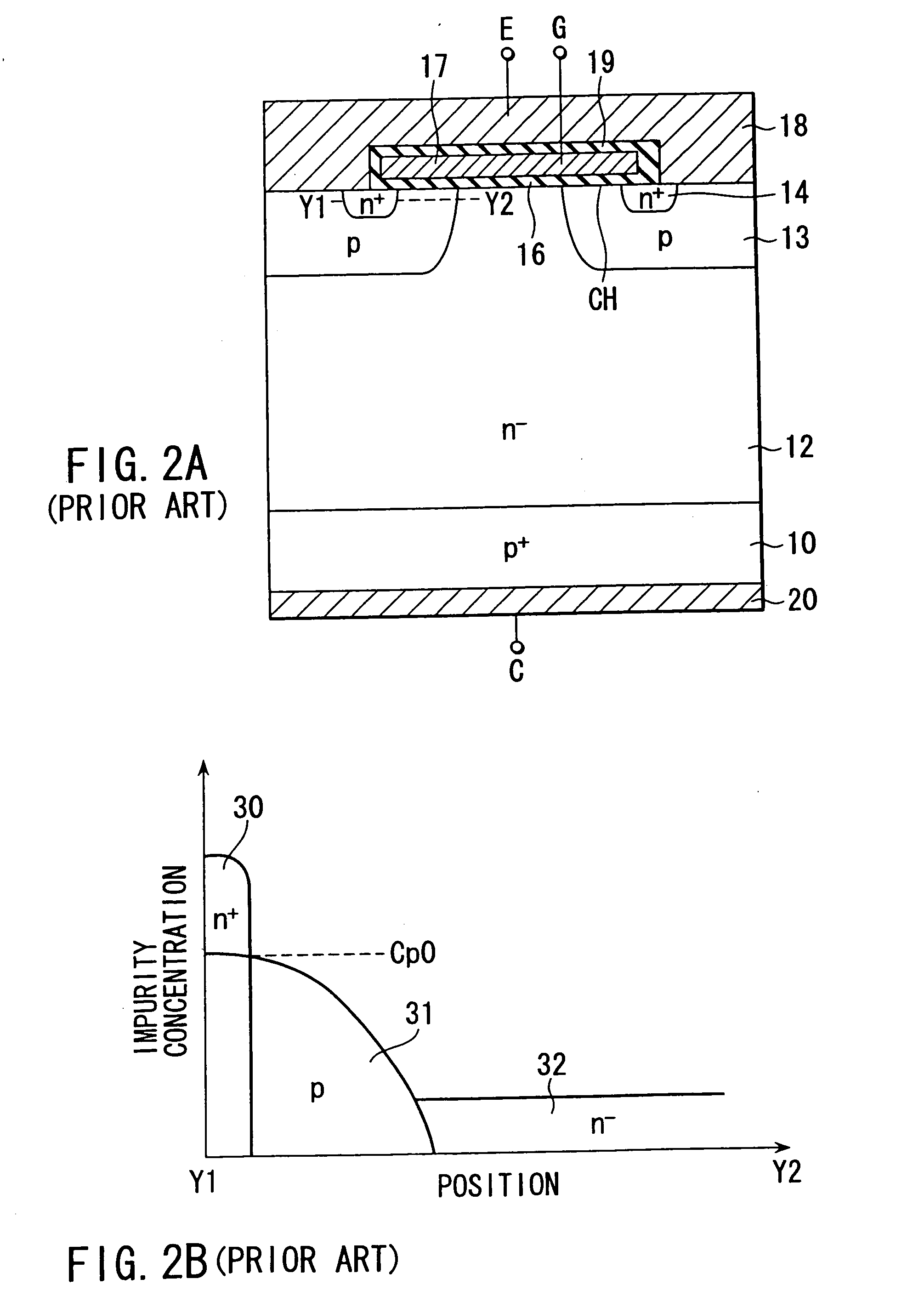
[0132]FIG. 3A is a cross sectional view schematically showing the construction of a trench IGBT, which is a power semiconductor element according to the present invention.
[0133] As shown in the drawing, an n+-type buffer layer 41, an n−-type base layer 42 having a high resistivity, a p+-type base layer 51 having a high impurity concentration, and a p-type base layer 43 having a low impurity concentration are formed in the order mentioned on one surface region of a p+-type collector layer 40. Also, an n+-type emitter layer 44 is selectively formed in a part of the surface region of the p-type base layer 43. Further, a trench 45 is formed to extend downward from the surface of the emitter layer 14 to reach the n−-type base layer 42 through the emitter layer 44, the p-type base layer 43 and the p+-type base layer 51. A gate electrode 47 (trench-gate electrode), which is covered with a gate insulating film 46, is buried in the trench 45. Incidentally, the emitter layer 44 is formed to h...
second embodiment
[0135] Incidentally, each of the trench-gate electrode 47 is formed to extend to reach, for example, a gate contact pad (not shown), and a gate electrode wiring is formed in contact with the gate contact pad. Also, a collector electrode 50 is formed on the back surface of the p+-type collector layer 40. Incidentally, the n+-type buffer layer 41 is intended to improve the breakdown voltage of the IGBT. Where the required breakdown voltage can be maintained by another method, it is possible to omit the n+-type buffer layer 41. This is also be case with the second embodiment, et seq. which are to be described herein later.
[0136] A MOSFET is formed of the n−-type base layer 42, the p+-type base layer 51, the p-type base layer 43, the emitter layer 44, the gate insulating film 46 and the trench-gate electrode 47. In the MOSFET thus formed, electrons are injected from the emitter layer 44 into the n−-type base layer 42 through a channel region CH formed in those portions of the p+-type ba...
third embodiment
[0175] Incidentally, the third embodiment is featured in that the p+-type base layer 51 having an impurity concentration higher than that in the p+-type base layer 43 is formed within the p+-type base layer 43. Such being the situation, it is possible to permit the p+-type base layer 51 to be present only in the vicinity of the trench 45 in a manner to be isolated from the n-type base layer 42 and in contact with the trench 45. In this case, the impurity concentration profile along the line X7-X8 is as shown in FIG. 4B, FIG. 4D or FIG. 4F.
[0176] A power semiconductor element according to a fourth embodiment of the present invention will now be described with reference to FIG. 6, which is a cross sectional view showing a trench IGBT. The trench IGBT according to the fourth embodiment is substantially equal to that according to the first embodiment, except that the trench IGBT of the fourth embodiment is allowed to have a trench contact structure.
[0177] As shown in FIG. 6, a trench 5...
PUM
 Abstract
Description
Claims
Application Information