Exposure apparatus and exposure method

a technology of exposure apparatus and exposure method, which is applied in the direction of microlithography exposure apparatus, printers, instruments, etc., can solve the problems of increased steps and costs of the manufacturing process of the reticle, increased cost of manufacturing the microdevice etc., and achieves high accuracy. fidelity

Inactive Publication Date: 2005-03-24
NIKON CORP
View PDF12 Cites 24 Cited by
  • Summary
  • Abstract
  • Description
  • Claims
  • Application Information

AI Technical Summary

Benefits of technology

[0015] The present invention was made in consideration of these problems in the prior art and has as its object to provide an exposure apparatus and an exposure method enabling the formation of fine patterns of the targeted line widths with a high accuracy (fidelity) without the amount of exposure at an overlay part becoming insufficient and without the occurrence of a change in the amount of exposure at an overlay part sensitive to positional error of the shots even when changing the illumination conditions.
[0017] If changing the illumination conditions, as explained above, the widths of the peripheral parts where the cumulative amount of energy is set at a slant change and the cumulative amounts of energy at the overlay parts where the peripheral parts overlap with other peripheral parts adjoining them will not become the desired value. As opposed to this, in the present invention, even if the illumination conditions are changed, the widths of the peripheral parts are kept from changing by correction by the correction device, so even if changing the illumination conditions, the widths of the overlay parts can be set to the desired value. Therefore, there will no longer be cases where the cumulative amount of energy becomes partially insufficient in an overlay part or the amount of energy at an overlay part changes sensitively with respect to positional error of the areas where the patterns are transferred and the cumulative amounts of energy at the overlay parts can be uniformly set to the desired value. As a result, it is possible to form fine patterns of the targeted line widths with a high accuracy and fidelity.
[0021] The correction device may correct the widths of the peripheral parts without changing the position of the setting device or, along with this, adjusting the optical characteristics of the optical elements arranged on the path of the energy beam from the setting device to the patterns.

Problems solved by technology

In such an exposure apparatus, there was sometimes misalignment in stitched portions of shots due to aberration of the projection optical system, positioning error of the reticle or substrate, etc.
Due to the formation of the light-attenuating parts in the reticle itself, however, the steps and cost of the manufacturing process of the reticle increase and the cost of manufacturing the microdevice etc. increase.
Therefore, if even a slight offset in position of the shots occurs, the amount of exposure of the overlay part for the offset will change greatly and as a result the change in line width will become sensitive to the offset.
However, part of the overlay part will be enlarged outside of the exposure area and that part outside of the exposure area will end up being blocked by a light-blocking strip formed at the reticle.
In this way, in the past, there was the problem that if for example changing the illumination σ or other illumination conditions to improve the OPE characteristic, the amount of change in the combined amount of exposure of an overlay part with respect to offset of the shots became greater and there was a susceptibility to changes in line width and also locations arose where the combined amount of exposure in the overlay part became insufficient and changes in line width occurred in the overlay part.

Method used


Image

  • Exposure apparatus and exposure method
  • Exposure apparatus and exposure method
  • Exposure apparatus and exposure method

Examples


Embodiment Construction

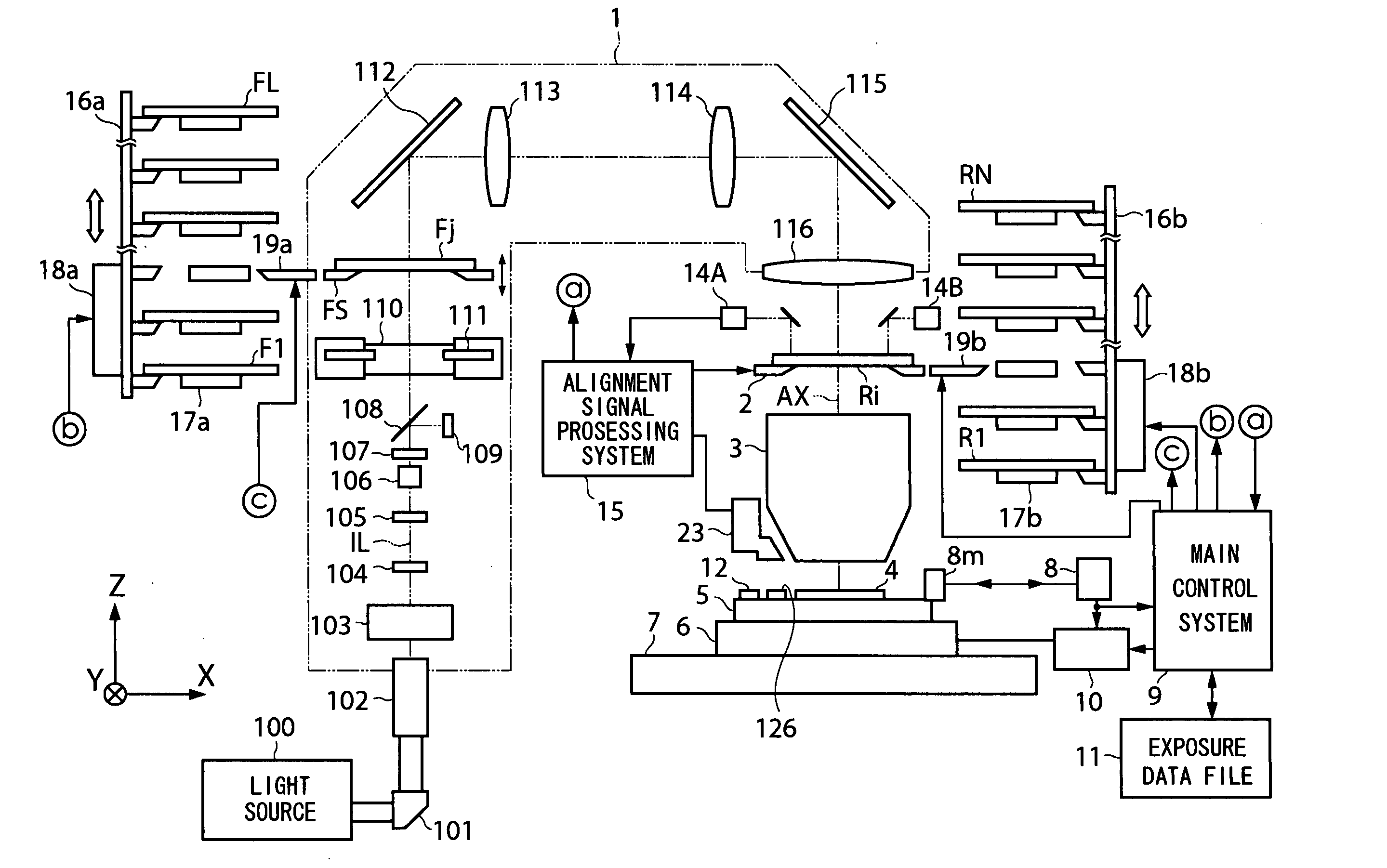
[0044] Below, an explanation will be given of an embodiment of the present invention with reference to the drawings. FIG. 1 is a view of the general configuration of an exposure apparatus according to an embodiment of the present invention. The exposure apparatus is a step-and-repeat type stitch projection exposure apparatus. Further, in the following explanation, the XYZ orthogonal coordinate system shown in FIG. 1 is set and the positional relationships of the members explained while referring to the XYZ orthogonal coordinate system. The XYZ orthogonal coordinate system is set so that the X-axis and the Z-axis become parallel to the paper surface and so that the Y-axis becomes the direction perpendicular to the paper surface. Further, the XYZ coordinate system in the figure is set so that the XY plane becomes a plane parallel to the horizontal surface and the Z-axis becomes the vertical direction.

[0045] In FIG. 1, the ultraviolet pulse light IL of the light from a light source 10...


PUM

PropertyMeasurementUnit
wavelengthaaaaaaaaaa
sizeaaaaaaaaaa
sizeaaaaaaaaaa

Abstract

Fine patterns with the targeted line widths are formed with a high accuracy by correcting any change in image of a light-attenuating part of a density filter on a substrate arising along with a change in illumination conditions on a reticle by adjusting an amount of defocus of the density filter with respect to a reticle conjugate plane.

Description

TECHNICAL FIELD [0001] The present invention relates to an exposure apparatus and exposure method used when producing a semiconductor integrated circuit, a liquid crystal display, a thin film magnetic head, or another microdevice or a photomask by photolithography. BACKGROUND ART [0002] In photolithography, one step in the production of a microdevice, use is made of an exposure apparatus for projection exposure of images of patterns of a photomask or reticle (hereinafter referred to generally as a “reticle”) on to a substrate for exposure (semiconductor wafer or glass plate coated with a photoresist, light-transparent substrate called a “blank”, etc.) In recent years, to deal with the increasingly large size of the exposure area accompanying the increased size of substrates, a stitching type exposure apparatus which partitions the exposure area of the substrate into a plurality of unit areas (hereinafter sometimes referred to as “shots” or “shot areas”) and successively projects and...

Claims


Application Information

Patent Timeline
Patent Type & Authority Applications(United States)
IPC IPC(8): G03F7/20
CPCG03F7/70066G03F7/701G03F7/70483G03F7/70216G03F7/70475G03F7/70191G03F7/70441
Inventor IRIE, NOBUYUKI
Owner NIKON CORP
Why Eureka
Try Eureka