Method of manufacturing wafer level chip size package

a technology of chip size and manufacturing method, which is applied in the direction of electrical equipment, semiconductor devices, semiconductor/solid-state device details, etc., can solve the problems of deteriorating operation efficiency, too much labor hour and time, and excessive time for forming, so as to improve operation efficiency

Inactive Publication Date: 2005-03-24
MINAMI
View PDF21 Cites 9 Cited by
  • Summary
  • Abstract
  • Description
  • Claims
  • Application Information

AI Technical Summary

Benefits of technology

[0008] The present invention is made by taking the points mentioned above into consideration, and an object of the present invention is to provide a method of manufacturing a wafer level chip size package (CSP) which can widely improve an operation efficiency.

Problems solved by technology

However, there is a problem that too much labor hour and time are required for forming the insulating layer 105 and the solder bump 106, and an operation efficiency is deteriorated.
Further, in the conventional structure, since the thermal stress relaxing layer 101 is made of the insulating material, it is necessary to form the land 102 in a center of a top surface thereof, so that there is a problem that an excess time is required for forming.

Method used


Image

  • Method of manufacturing wafer level chip size package
  • Method of manufacturing wafer level chip size package

Examples


Embodiment Construction

[0019] A description will be given below of an embodiment in accordance with the present invention with reference to the accompanying drawing.

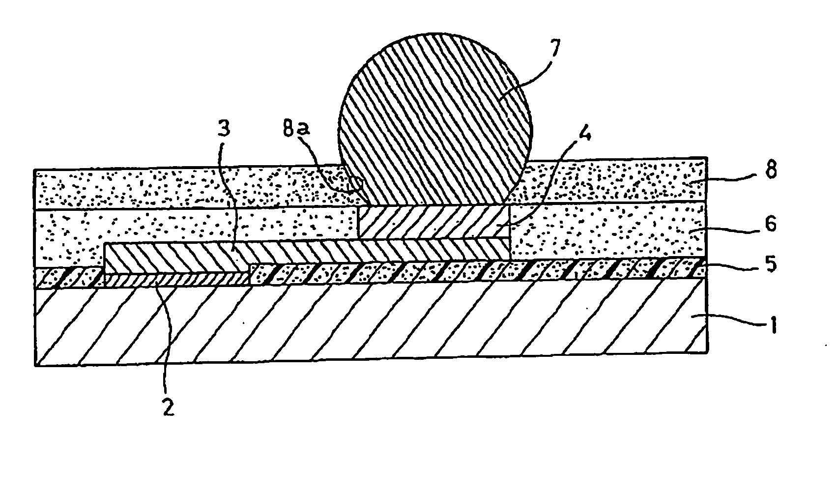
[0020]FIG. 1 is a view showing a cross section of a wafer level chip size package (CSP) manufactured in accordance with the present invention.

[0021] In the drawing, reference numeral 1 denotes a wafer. Reference numeral 2 denotes a bonding pad formed on the wafer 1. The bonding pad 2 is a gold UBM. Reference numeral 3 denotes a rewiring circuit formed on the wafer 1 in accordance with a plating process. Reference numeral 4 denotes a thermal stress relaxing post formed on the rewiring circuit 3 and made of a conductive material such as a solder or the like. The thermal stress relaxing post 4 is formed in accordance with a screen printing process by a pressure type screen printing machine. In this case, a solder is used as the conductive material.

[0022] Reference numeral 5 denotes an insulating layer formed on the wafer 1, and reference numer...


PUM


Abstract

To widely improve an entire manufacturing efficiency by efficiently forming a thermal stress relaxing post, an insulating layer and a solder bump, a rewiring circuit (3) is formed on a wafer (1) by plating, a thermal stress relaxing post (4) made of a conductive material such as a solder or the like is formed on the rewiring circuit (3), an insulating layer (6) made of a polyimide or the like is formed in the periphery of the rewiring circuit (3) and the thermal stress relaxing post (4) except a top surface of the thermal stress relaxing post (4), a solder bump (7) is formed on the thermal stress relaxing post (4), and the thermal stress relaxing post (4), the insulating layer (6) and the solder bump (7) are formed by screen printing.

Description

BACKGROUND OF THE INVENTION [0001] 1. Field of the Invention [0002] The present invention relates to a method of manufacturing a wafer level chip size package. [0003] 2. Description of the Prior Art [0004] On the basis of a demand for high density mounting in a cellular phone, a digital video, a digital camera and the like, the chip size package (CSP) corresponding to a compact package is going to become rapidly popular. [0005] In the CSP, since a mounting area is smaller and a wiring length is shorter in comparison with a conventional lead type package such as a thin small outline package (TSOP) and a quad flat package (QFP), there is a characteristic that the CSP is easily applied to a high-frequency device. Further, in comparison with a flip chip in which a chip is directly mounted on a substrate, since it is possible to widen a pad pitch, there is a characteristic that it is easy to mount on the substrate. In other words, the CSP is becoming rapidly popular because it is possibl...

Claims


Application Information

Patent Timeline
Patent Type & Authority Applications(United States)
IPC IPC(8): H01L21/60H01L23/31H01L23/48H01L23/12H01L23/485
CPCH01L23/293H01L2924/0002H01L23/3192H01L23/525H01L23/562H01L24/03H01L24/05H01L24/11H01L24/13H01L2224/0236H01L2224/0332H01L2224/0401H01L2224/05567H01L2224/05569H01L2224/056H01L2224/1132H01L2224/13022H01L2224/131H01L2924/01004H01L2924/01006H01L2924/01075H01L2924/01078H01L2924/01079H01L2924/01082H01L2924/01327H01L2924/014H01L23/3114H01L2224/024H01L2924/01033H01L2224/05552H01L2924/351H01L2924/00H01L23/48
Inventor MURAKAMI, TAKEHIKO
Owner MINAMI
Why Eureka
Try Eureka