Sacrificial surfactanated pre-wet for defect reduction in a semiconductor photolithography developing process

a technology of semiconductor photolithography and surfactanated prewet, which is applied in the direction of photosensitive materials, instruments, photomechanical equipment, etc., can solve the problems of high contact angle between the photoresist surface and liquid to capture small air bubbles, and achieve the effect of unfavorable chemical reactions

Inactive Publication Date: 2005-03-31
TOKYO ELECTRON LTD
View PDF12 Cites 8 Cited by
  • Summary
  • Abstract
  • Description
  • Claims
  • Application Information

AI Technical Summary

Benefits of technology

[0008] In the method for the developing process according to the present invention, it is possible to carry out the developing process by using a developing solution having an appropriate concentration conforming to the characteristics of the resist film and the surfactant-containing layer relative to the developing solution. Further, since the displacement of the surfactant-containing layer with developing liquid precludes the defect causing mechanism of high contact angle, it is possible to obtain a circuit pattern with fewer defects related to that mechanism.
[0009] According to the present invention, provided is an apparatus for supplying a surfactant-containing liquid and a developing solution, which can be suitably employed in the method of the present invention for the developing process described above. Additionally, the present invention addresses the fundamental problem of high developing liquid contact angle directly by using a sacrificial surfactanated pre-wet step prior to supplying developing solution to the wafer surface. The pre-wet can be a material that is compatible with the developing chemical; however, it will have surfactant added to provide a uniform defect-free liquid film on the surface. Because the sacrificial pre-wet is not a process active chemical, other concerns are minimized, such as undesired chemical reactions. This non-active, defect-free film is displaced by the dispensing of the actual developing process chemical. The balance of the developing process is carried out as described in the Background of the Invention. By this approach, the defect mechanism of the high developing liquid contact angle on the resist surface is substantially, if not completely, avoided.

Problems solved by technology

Under these circumstances, it is difficult to form a defect-free circuit pattern by the conventional method for the developing process.
This combination results in a high contact angle between the photoresist surface and the spreading developing liquid.
This high contact angle opposes uniform spreading of the developing liquid and can cause the liquid to capture small air bubbles (microbubbles).
These approaches have had limited success.
The complex mechanisms and spin / dispense recipes are difficult to program and control repeatably, and they do not resolve the fundamental problem of high contact angle.

Method used


Image

  • Sacrificial surfactanated pre-wet for defect reduction in a semiconductor photolithography developing process
  • Sacrificial surfactanated pre-wet for defect reduction in a semiconductor photolithography developing process
  • Sacrificial surfactanated pre-wet for defect reduction in a semiconductor photolithography developing process

Examples


Embodiment Construction

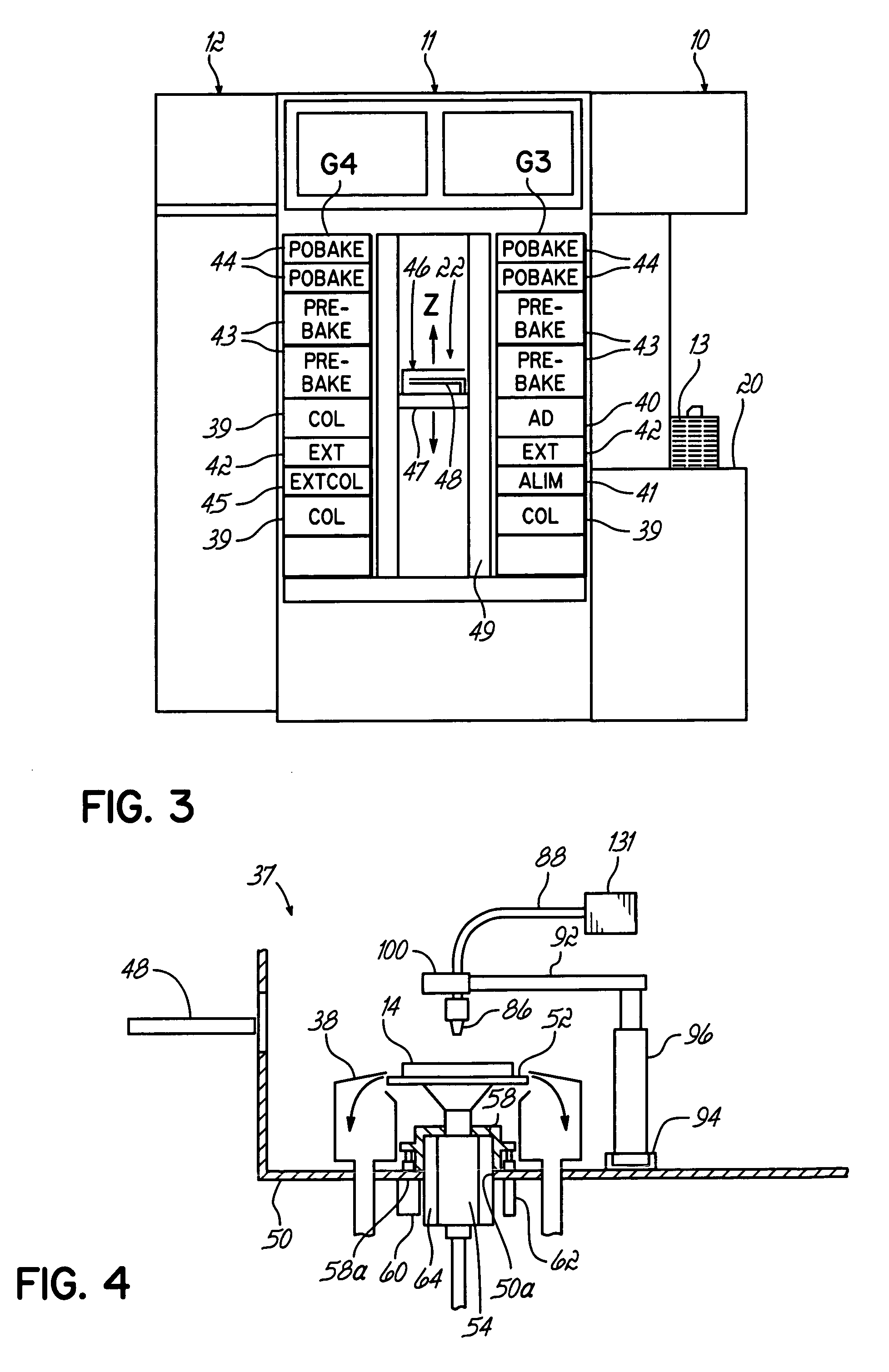
[0018] The method of the present invention includes the addition of a process step prior to the developing solution dispensing step in the developing process of a semiconductor photolithography process, followed by a modified developing dispensing step. The added process step is the dispensing of a sacrificial surfactant-containing liquid onto the surface of a photoresist coated semiconductor wafer, such as a silicon wafer, to form a defect-free liquid film on that surface. This film is subsequently displaced by a slightly modified developing solution dispensing step to achieve a uniform defect-free layer of developing solution on the surface of the wafer.

[0019] For example, the added process step may comprise dispensing a sacrificial layer of deionized water to which a non-contaminating surfactant has been added, to thereby form a defect-free liquid film on the wafer surface. This film is subsequently displaced by dispensing a tetramethylammonium hydroxide (TMAH)-based developing ...


PUM

PropertyMeasurementUnit
widthaaaaaaaaaa
concentrationaaaaaaaaaa
contact angleaaaaaaaaaa

Abstract

A method and apparatus for developing a resist on a substrate in which a sacrificial surfactant-containing liquid is first applied to a resist as a pretreatment to reduce developing process defects and to improve the development process time and the uniformity of the resist. The pretreatment is followed by supplying a developing solution to the resist and thereafter developing the resist.

Description

FIELD OF THE INVENTION [0001] The present invention relates to a method for a developing process of a substrate such as a semiconductor wafer subjected to an exposure treatment, and an apparatus for supplying a surfactant-containing liquid and a developing solution. BACKGROUND OF THE INVENTION [0002] In a manufacturing process of a semiconductor device, a prescribed circuit pattern is formed on the surface of a semiconductor wafer by using a so-called “photolithography technology”. In the photolithography step, a series of treatments are carried out such that a resist film is formed on a cleaned semiconductor wafer by supplying a photoresist solution onto the semiconductor wafer, followed by exposing the resist film to light in a prescribed pattern and subsequently developing the pattern. [0003] In the developing step, an exposed semiconductor wafer is held first by a rotatable spin chuck. Then, a puddle of a developing solution is formed by supplying a developing solution onto the ...

Claims


Application Information

Patent Timeline
Patent Type & Authority Applications(United States)
IPC IPC(8): G03F7/30G03F7/32
CPCG03F7/322
Inventor KULP, JOHN M.
Owner TOKYO ELECTRON LTD
Why Eureka
Try Eureka