Check patentability & draft patents in minutes with Patsnap Eureka AI!

High power light emitting diode device

a light-emitting diode, high-power technology, applied in semiconductor devices, semiconductor/solid-state device details, electrical apparatus, etc., can solve the problems of reduced led efficiency, excessive heat generation of high drive currents, and light output dropping, so as to facilitate heat transfer

Inactive Publication Date: 2005-04-14
AVAGO TECH ECBU IP (SINGAPORE) PTE LTD
View PDF4 Cites 72 Cited by
  • Summary
  • Abstract
  • Description
  • Claims
  • Application Information

AI Technical Summary

Benefits of technology

[0006] The first trace preferably includes a solder ball on the first portion thereof. The circuit element may include a second trace for making the connection to the second contact point on the die. Alternatively, the second connection can be made through the heat-conducting die itself. A second solder ball is preferably placed on the second trace or the heat-conducting body to provide an electrical connection to the second contact point of the die. A third solder ball is preferably provided on the top surface of the heat conducting body at a location that is non-colinear with the first and second solder balls. The solder balls provide a mechanism for coupling the circuit element to a printed circuit board as well as providing power to the die. To further facilitate heat transfer from the heat-conducting body, the bottom surface of the heat conducting body may include fins or other features for increasing the surface area of the bottom surface relative to the top surface of the heat conducting body.

Problems solved by technology

Unfortunately, such high drive currents produce excessive heat.
Since the efficiency of an LED decreases at these high temperatures, light output starts to drop.
In addition, the packaging of the devices starts to break down due to prolonged exposure to the elevated temperatures.
Such packaging failures limit useful life of the device.
A number of device packages have been proposed; however, none of these provide sufficient heat dissipation for the current generation of high-power LEDs.

Method used


Image

  • High power light emitting diode device
  • High power light emitting diode device
  • High power light emitting diode device

Examples


Embodiment Construction

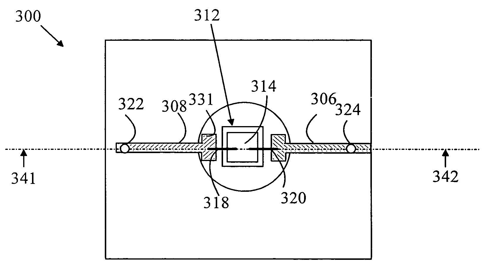
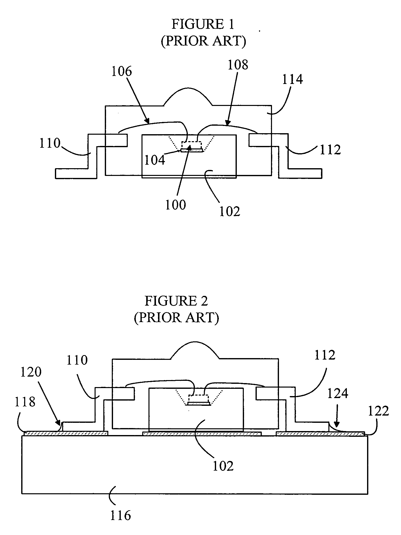
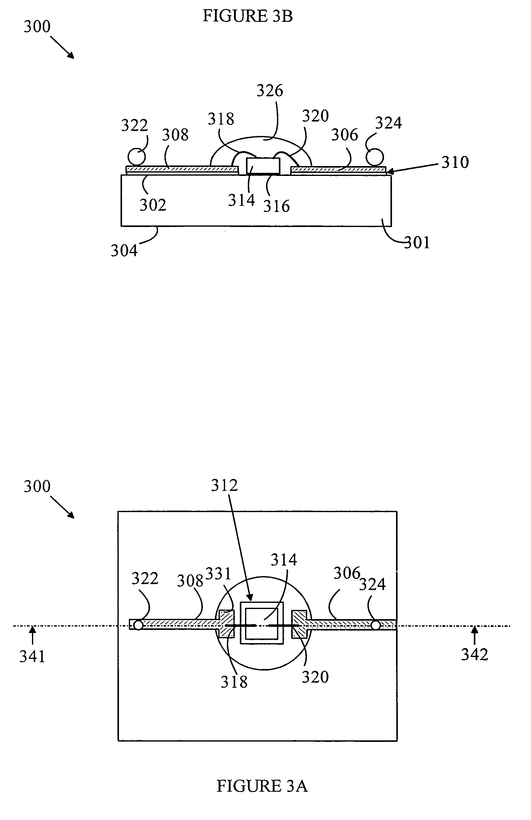
[0018] The manner in which the present invention provides its advantages can be more easily understood with reference to FIGS. 1 and 2, which illustrate the manner in which one class of prior art LED provides heat dissipation. Refer now to FIG. 1, which is cross-sectional view of a packaged LED according to one prior art design. An LED 100 is mounted in a cavity of a substrate 102 using a conductive medium 104. A first bond wire 106 electrically connects one terminal of the LED 100 to one electrical contact 110 while a second bond wire 108 electrically connects a second terminal of LED 100 to another electrical contact 112. An encapsulating body 114 substantially encases the LED, the bond wires, the substrate and the contacts to provide protection for the LED.

[0019] Refer now to FIG. 2, which is a cross-sectional view of the packed LED shown in FIG. 1 attached to a typical printed circuit board (PCB) 116. The base of substrate 102 is mounted on a PCB 116 so that it is in direct con...


PUM


Abstract

A circuit element having a heat-conducting body having top and bottom surfaces, and a die having an electronic circuit thereon is disclosed. The die includes first and second contact points for powering the electronic circuit. The die is in thermal contact with the heat-conducting body, the die having a bottom surface that is smaller than the top surface of the heat-conducting body. The first contact point on the die is connected to a first trace bonded to the top surface of the heat-conducting body. An encapsulating cap covers the die. The first trace has a first portion that extends outside of the encapsulating cap and a second portion that is covered by the encapsulating cap. The heat-conducting body is preferably constructed from copper or aluminum and includes a cavity having an opening on the first surface in which the die is mounted. The die preferably includes a light-emitting device.

Description

FIELD OF THE INVENTION [0001] The present invention relates to packaged integrated circuits, and more particularly, to high-power LEDs. BACKGROUND OF THE INVENTION [0002] Light emitting diodes (LEDs) are fabricated from compound semiconductor materials, which have the characteristic of emitting light when biased with a forward current. LEDs are widely used as indicators or displays in various types of appliances. Historically, LEDs emitted a relatively low level of light compared to other light sources and were suitable for indoor applications only. [0003] Recent advances in compound semiconductor materials research have yielded new LEDs, which emit very high levels of light. Examples of these new LED materials are Aluminum Indium Gallium Phosphide (AlInGaP) and Indium Gallium Nitride (InGaN). These high brightness LEDs have given rise to new LED devices suitable for applications in areas such as outdoor video displays, automotive signals, traffic signals and illumination. [0004] Th...

Claims


Application Information

Patent Timeline
IPC IPC(8): H01L23/36H01L33/62H01L33/64
CPCH01L23/36H01L2924/12041H01L33/64H01L2224/48091H01L2224/48247H01L2224/49175H01L2224/73265H01L2924/14H01L2924/15311H01L2924/1532H01L33/62H01L2924/01068H01L2224/32245H01L24/49H01L24/48H01L2224/32257H01L2924/00014H01L2924/00H01L2924/181H01L2924/1815H01L2924/00012H01L2224/45099H01L2224/45015H01L2924/207H01L23/34H01L23/48
Inventor NG, KEE YEANTAN, CHENG WHYTHAM, JI KIN
Owner AVAGO TECH ECBU IP (SINGAPORE) PTE LTD
Features
  • R&D
  • Intellectual Property
  • Life Sciences
  • Materials
  • Tech Scout
  • Unparalleled Data Quality
  • Higher Quality Content
  • 60% Fewer Hallucinations
Learn More