

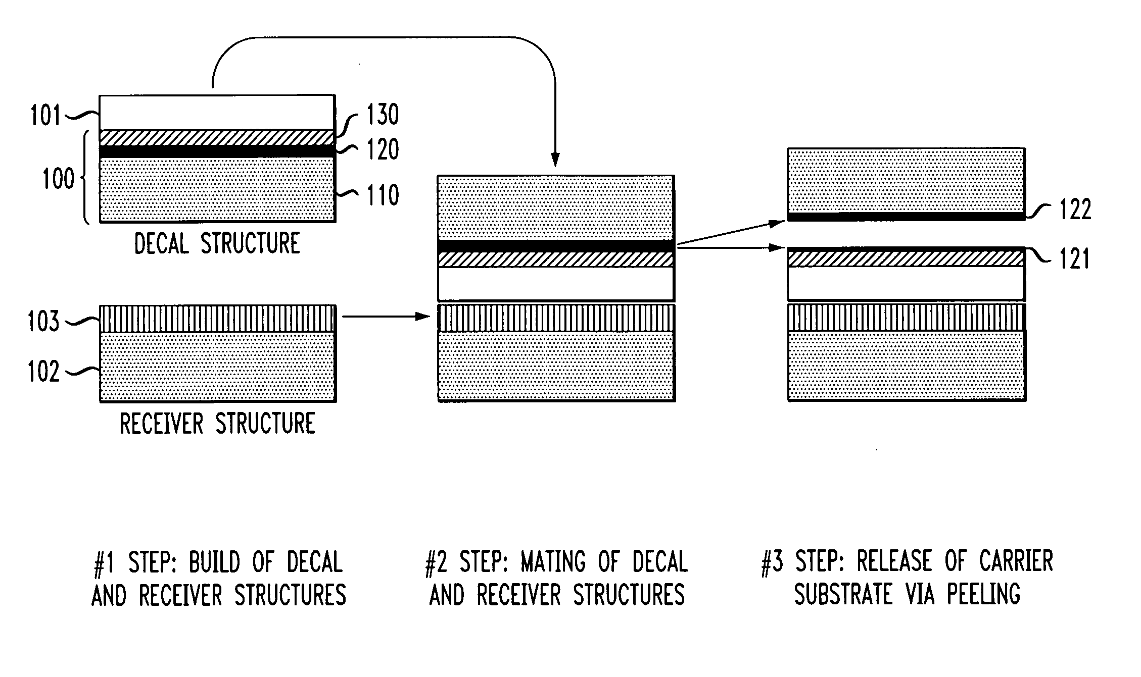
Techniques for layer transfer processing
- Summary
- Abstract
- Description
- Claims
- Application Information
AI Technical Summary
Problems solved by technology
Method used
Image

Examples
example
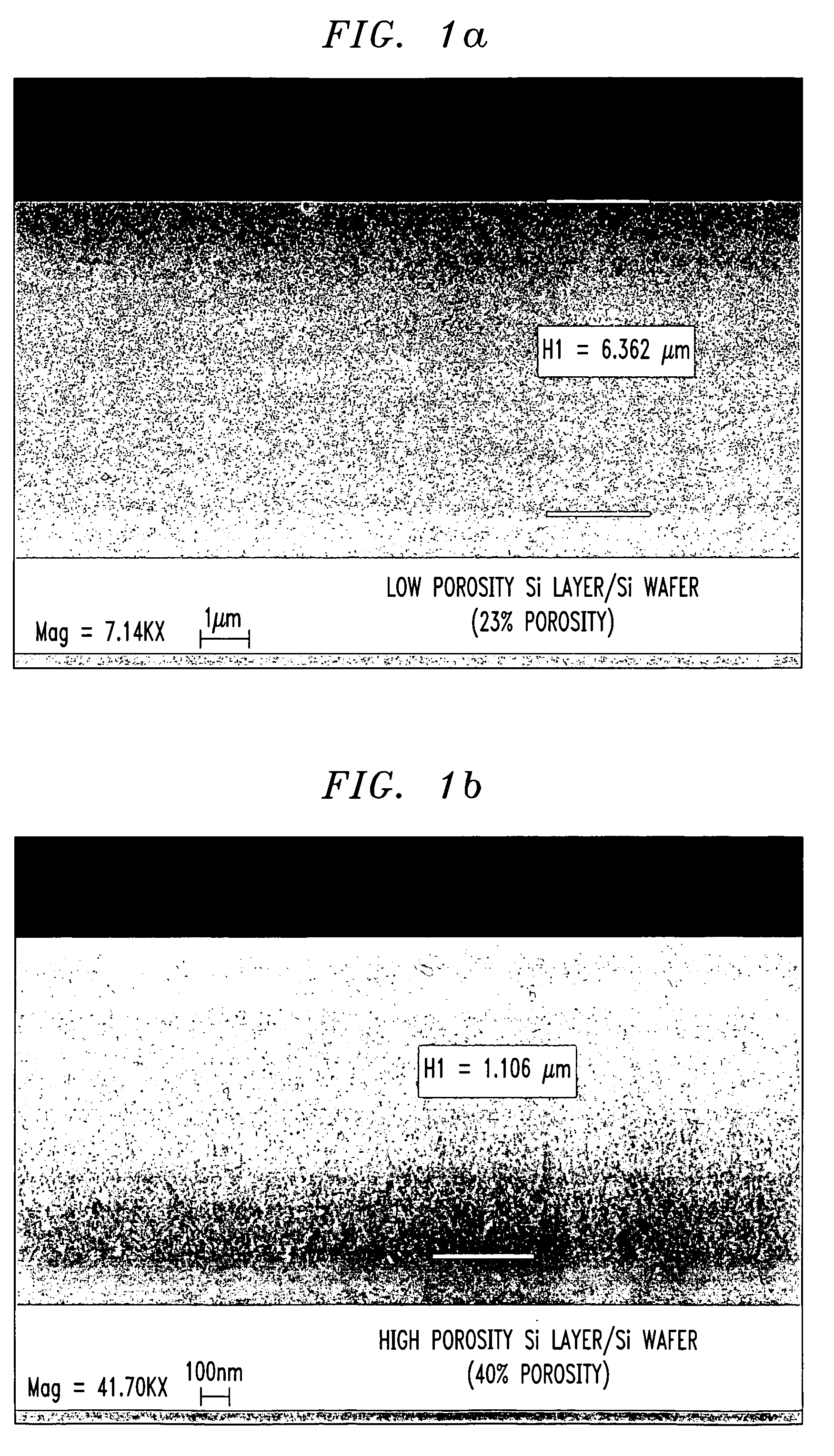
[0062] Method to create a separation layer using a combination of ion implantation and anodization:
Implantation of a Species into a Silicon Substrate:
[0063] Starting carrier substrate: boron-doped (about 1×1019 cm-3) silicon or substrate boron-doped (about 1×1019 cm-3) silicon with about two micrometers of undoped epitaxial silicon.
Process Steps:
[0064] 1. Implantation: boron, 160 to 220 kiloelectron volt (keV), 1-5×1016 cm-2, +silicon, 200 to 400 keV, 1×10¹⁵ to 1×1016 cm-2, preferred→160 keV B+, 2×1016 cm-2+silicon, 220 keV, 2×1015 cm-2.
[0065] 2. Boron electrical activation anneal: 550 to 800° C. / 15 minutes to 3 hours in a furnace or rapid thermal anneal (RTA) at 800 to 1100° C. / 5 to 500 seconds, preferred→650 / 165 minutes in a furnace.
[0066] 3. Anodization: with the Substrate as the positive electrode and a platinum plate as a negative electrode, current densities (0.05 to 50 milli Amps (mA) cm-2).
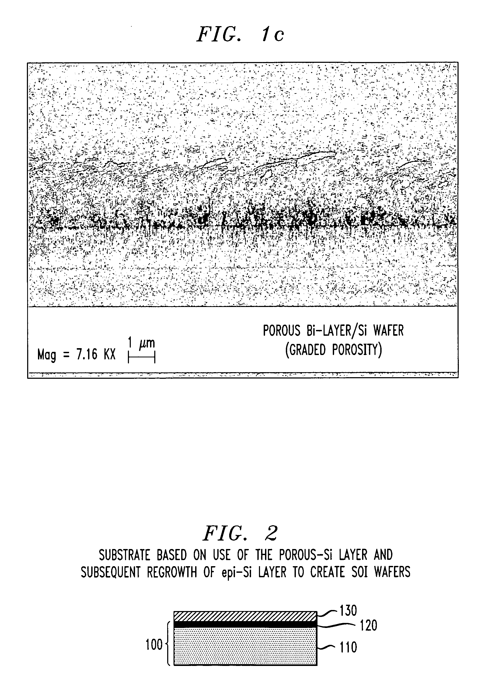
[0067] This process leads to a typical porous structure with an implant induc...
PUM
 Abstract
Description
Claims
Application Information