Liquid crystal display device

a liquid crystal display and display device technology, applied in static indicating devices, instruments, non-linear optics, etc., can solve the problems of increasing manufacturing costs and requiring a large space, and achieve the effect of narrow frame area, reducing the required area of the pcb, and reducing the non-display area

Inactive Publication Date: 2005-04-21
HANNSTAR DISPLAY CORPORATION
View PDF8 Cites 6 Cited by
  • Summary
  • Abstract
  • Description
  • Claims
  • Application Information

AI Technical Summary

Benefits of technology

[0008] The present invention provides a conductive line structure of a liquid crystal display, which comprises a liquid crystal panel for displaying the image, a glass substrate, Y-direction driver integrated circuit (IC) chips, X-direction driver integrated circuit (IC) chips, a Y-direction printed circuit board (Y-PCB) and an X-direction printed circuit board (X-PCB). The PCBs and are used to process the electrical signal. The driver IC chips are located on a first flexible printed circuit (FPC). The first FPC board can be a tape carrier package (TCP) or a chip on film (COF). The conductive lines in the present invention are all arranged in the first FPC board and the glass substrate to reduce the required area of the PCB. In other words, a liquid crystal display with a narrow frame area can be obtained by reducing the non-display area. Therefore, the volume and the weight of the liquid crystal display can be improved.

Problems solved by technology

Such structure not only requires a large space but also increases the manufacturing cost.

Method used


Image

  • Liquid crystal display device
  • Liquid crystal display device
  • Liquid crystal display device

Examples


first embodiment

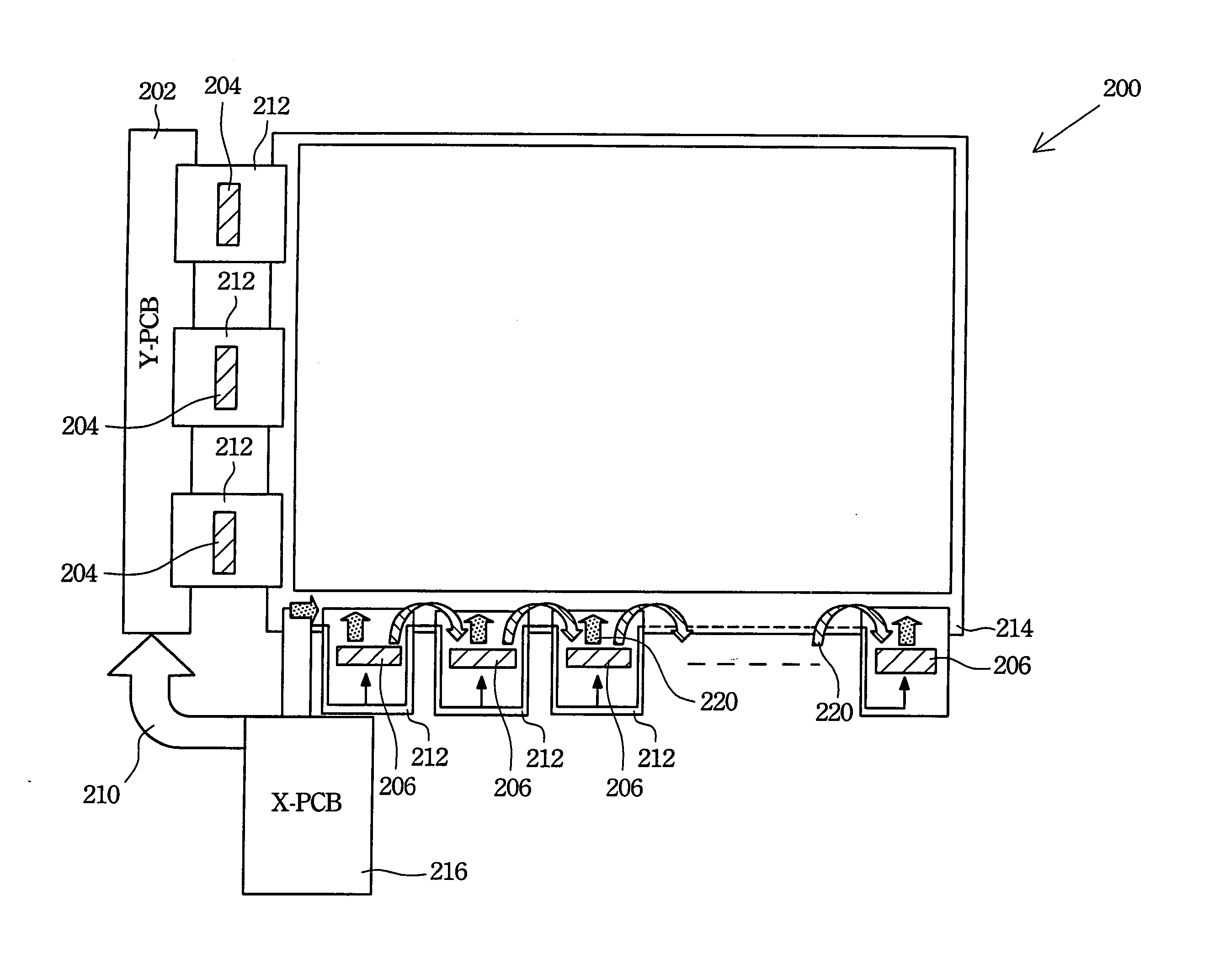
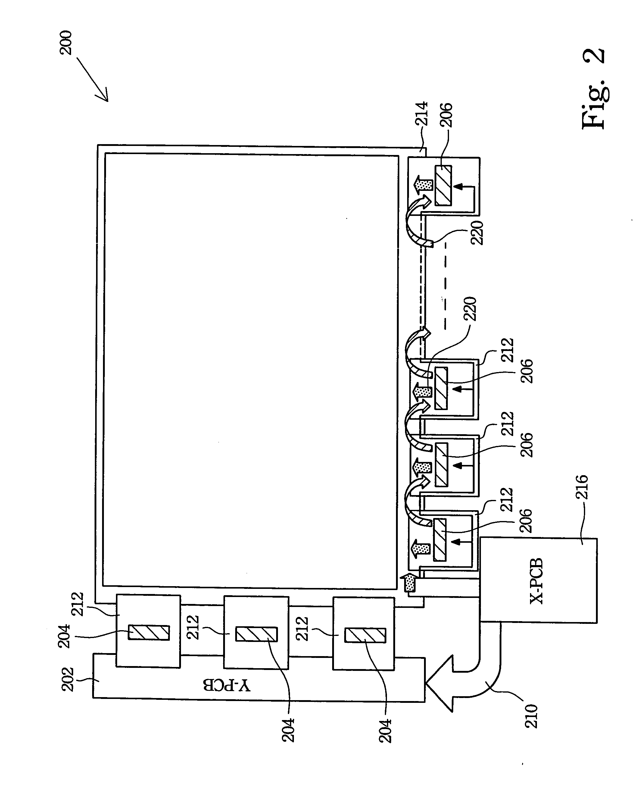
[0018]FIG. 2 illustrates a schematic diagram of a liquid crystal display according to the present invention, which comprises a liquid crystal panel 200 located on a glass substrate 214 for displaying the image, Y-direction driver integrated circuit (IC) chips 204, X-direction driver integrated circuit (IC) chips 206, a Y-direction printed circuit board (Y-PCB) 202 and an X-direction printed circuit board (X-PCB) 216. The PCBs 202 and 216 are used to process the electrical signal. The driver IC chips 204 and 206 are located on a flexible printed circuit (FPC) 212. The FPC board 212 can be a tape carrier package (TCP) or a chip on film (COF). An another printed circuit board 210 is used to connect the PCBs 202 and 216. The another printed circuit board 210 is a flexible printed circuit film.

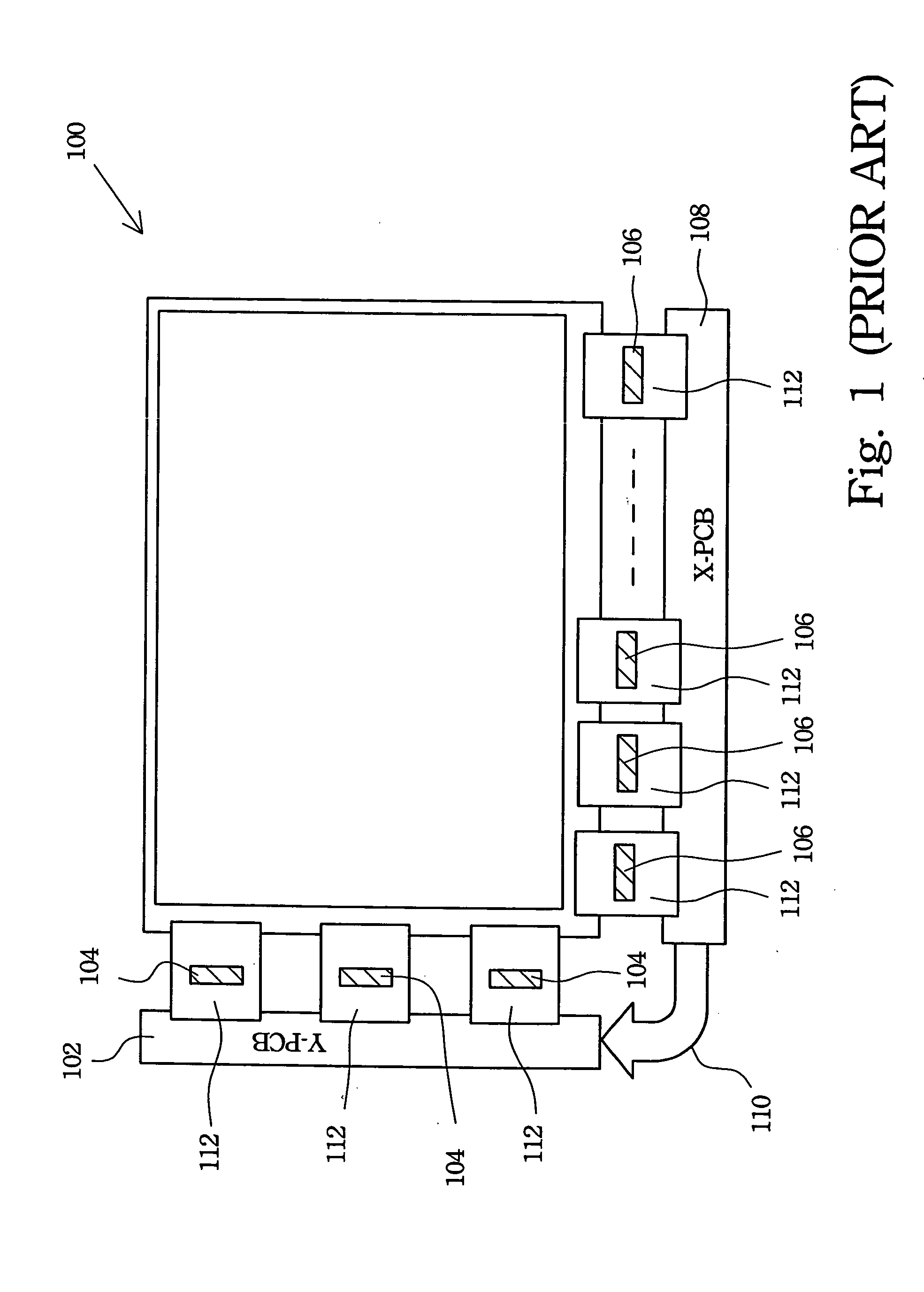
[0019] The conductive lines in the conventional structure are arranged in the X-direction PCB 108 as illustrated in the FIG. 1. However, the conductive lines in the present invention are arranged i...

second embodiment

[0026] Besides the above-mentioned method, the present invention also applies another method to solve power decay as shown in FIG. 5.

[0027]FIG. 5 illustrates a schematic diagram of a liquid crystal display according to the second embodiment of the present invention, which comprises a liquid crystal panel 200 located on a glass substrate 214 for displaying the image, Y-direction driver integrated circuit (IC) chips 204, X-direction driver integrated circuit (IC) chips 206, a Y-direction printed circuit board (Y-PCB) 202 and an X-direction printed circuit board (X-PCB) 230. The PCBs 202 and 230 are used to process the electrical signal. The driver IC chips 204 and 206 are located on a flexible printed circuit (FPC) 212. The FPC board 212 can be a tape carrier package (TCP) or a chip on film (COF). An another printed circuit board 210 is used to connect the PCBs 202 and 216. The another printed circuit board 210 is a flexible printed circuit film.

[0028] The conductive lines in the con...


PUM

PropertyMeasurementUnit
structureaaaaaaaaaa
flexibleaaaaaaaaaa
drain voltageaaaaaaaaaa

Abstract

The present invention provides a conductive line structure of a liquid crystal display. In accordance with this structure, the conductive lines in the present invention are all arranged in the FPC board and the glass substrate. Therefore, the required area of the PCB can be reduced, which also reduce the volume ands weight of the LCD.

Description

FIELD OF THE INVENTION [0001] The present invention relates to a liquid crystal display and more particularly to a liquid crystal display with narrow frame area by reducing the non-display area. BACKGROUND OF THE INVENTION [0002] With the merits of small volume and lightweight, liquid crystal display (LCD) holds the edge in the market for portable display devices and small-space application displays. Among all, the thin film transistor liquid crystal display (TFT-LCD) is the preferred device. A TFT-LCD uses field effect transistors to control the voltage applied to the liquid crystal film layer so as to control the orientation of liquid crystal molecules, thus adjusting the penetration of light through the liquid crystal layer. With the utilization of filters, a screen is able to display various colors and degrees if brightness. [0003]FIG. 1 illustrates the schematic diagram of a conventional liquid crystal display, which comprises a liquid crystal panel 100 for displaying the image...

Claims


Application Information

Patent Timeline
Patent Type & Authority Applications(United States)
IPC IPC(8): G02F1/13G02F1/1345G09G3/36
CPCG02F1/13452G09G2310/0283G09G2310/027G09G3/3688
Inventor HSU, CHIN-HUNG
Owner HANNSTAR DISPLAY CORPORATION
Why Eureka
Try Eureka