Semiconductor device and method for fabricating the same

a semiconductor device and semiconductor technology, applied in the direction of semiconductor devices, electrical devices, transistors, etc., can solve the problems of increasing micronization of semiconductor devices, reducing the mobility of carriers, and limiting the speed of semiconductor devices, so as to suppress the short channel effect, prevent surface scattering, and high mobility

Inactive Publication Date: 2005-04-21
FUJITSU LTD
View PDF7 Cites 8 Cited by
  • Summary
  • Abstract
  • Description
  • Claims
  • Application Information

AI Technical Summary

Benefits of technology

[0009] An object of the present invention is to provide a semiconductor device which can increase the carrier mobility while suppressing the short channel effect, and a method for fabricating the semiconductor device.
[0012] The present invention can prevent the surface scattering of carriers and the phonon scattering while suppressing the short channel effect. Thus, the present invention can provide a semiconductor device having high mobility and high speed.

Problems solved by technology

Then, recently, the semiconductor device is increasingly micronized.
The decrease of the carrier mobility has been a barrier to higher speed of the semiconductor device.

Method used


Image

  • Semiconductor device and method for fabricating the same
  • Semiconductor device and method for fabricating the same
  • Semiconductor device and method for fabricating the same

Examples


first embodiment

A FIRST EMBODIMENT

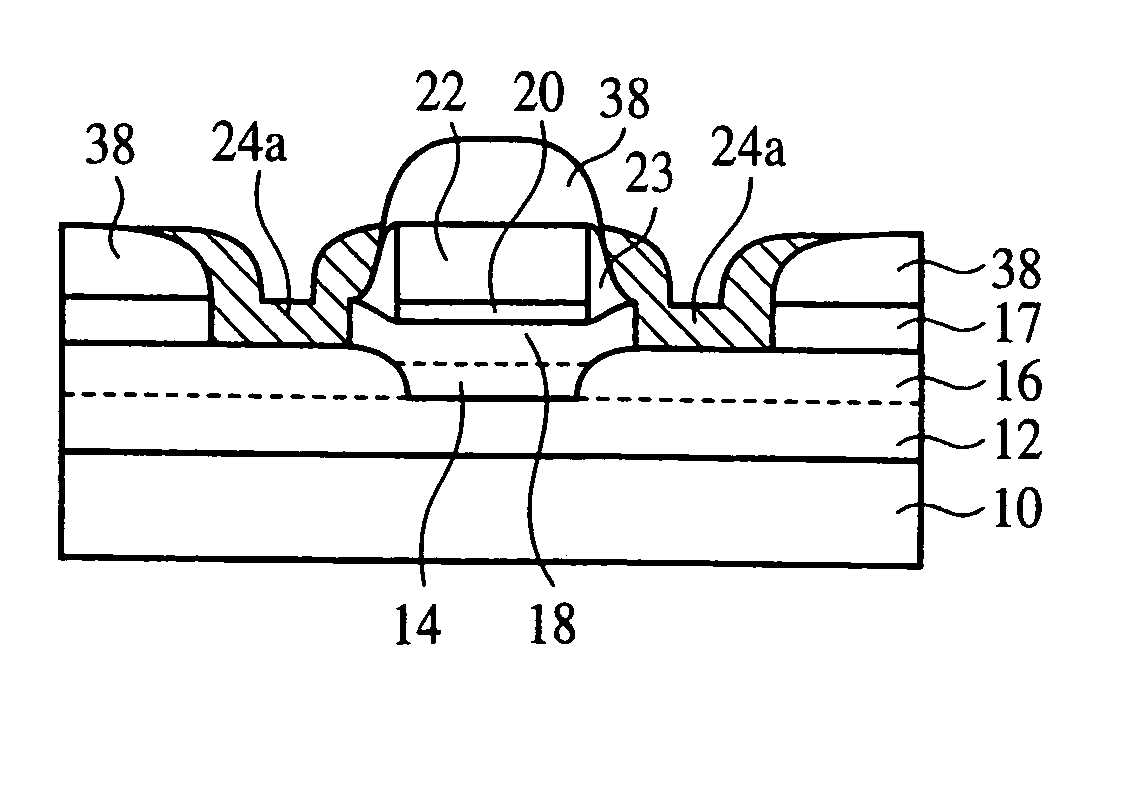
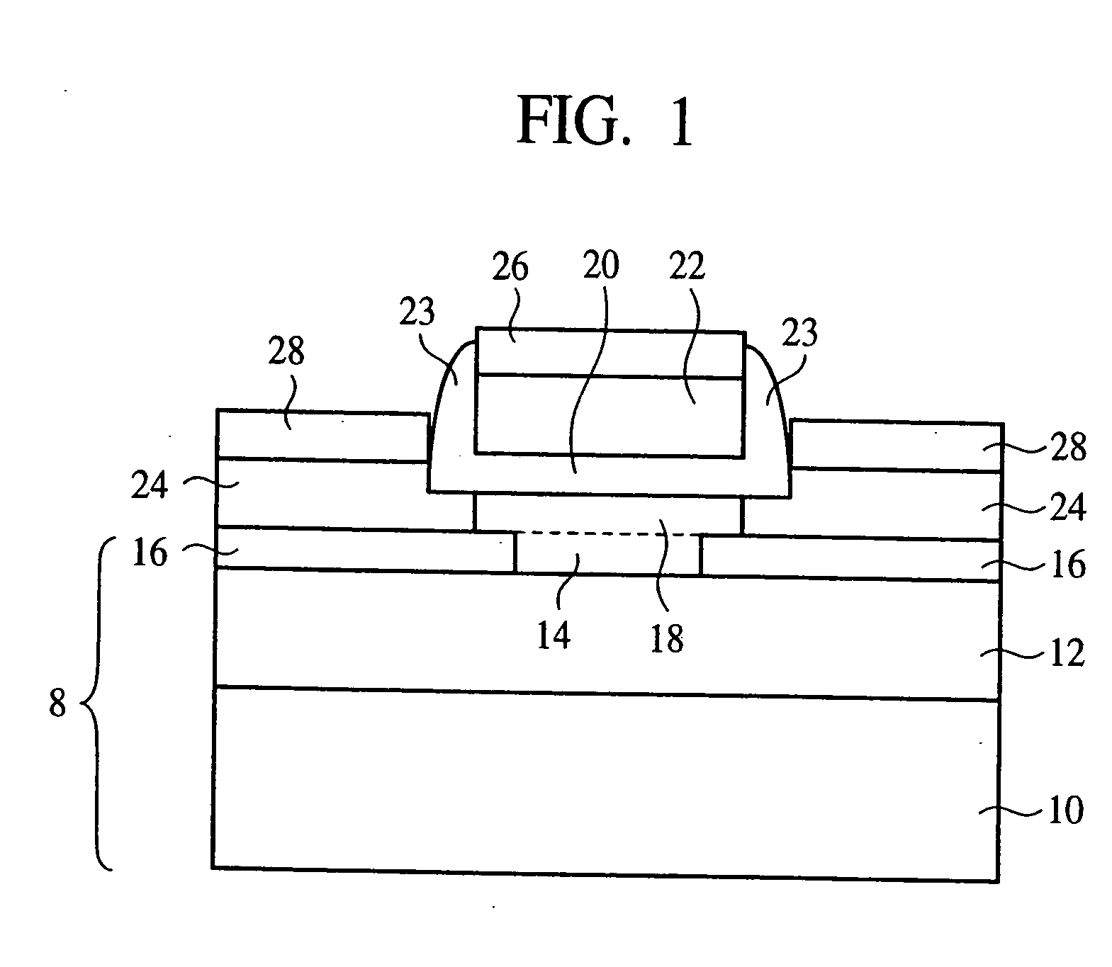
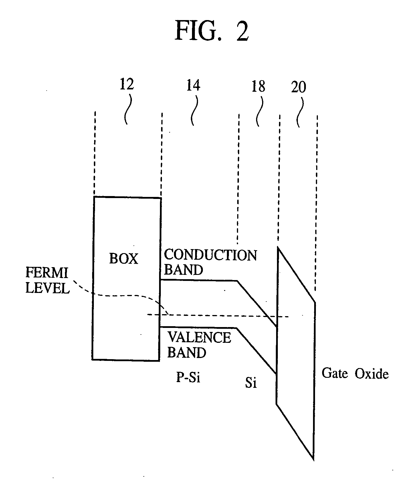
[0040] The semiconductor device according to a first embodiment of the present invention and a method for fabricating the semiconductor device will be explained with reference to FIGS. 1 to 5C. FIG. 1 is a sectional view of the semiconductor device according to the present embodiment.

[0041] (The Semiconductor Device)

[0042] First, the semiconductor device according to the present embodiment will be explained with reference to FIG. 1.

[0043] As shown in FIG. 1, an insulation film 12 of, e.g., 100 nm-thickness SiO2 is formed on a substrate 10 of silicon.

[0044] On the insulation film 12, a semiconductor region 14 of, e.g., a 20 nm-thickness p type Si. The semiconductor region 14 is single crystallized.

[0045] An insulation film 16 of SiO2 is formed on both sides of the semiconductor region 14. The insulation layer 16 is formed by oxidizing a semiconductor layer.

[0046] In the present embodiment, an SOI substrate 8 is used. The substrate 10 is the base substrate of t...

second embodiment

A SECOND EMBODIMENT

[0127] The semiconductor device according to a second embodiment of the present invention will be explained with reference to FIG. 15. FIG. 15 is a sectional view of the semiconductor device according to the present embodiment. The same members of the present embodiment as those of the semiconductor device according to the first embodiment and the method for fabricating the semiconductor device shown in FIGS. 1 to 14 are represented by the same reference numbers not to repeat or to simplify their explanation.

[0128] The semiconductor device according to the present modification is characterized mainly in that a semiconductor region 14a of Si is formed below the semiconductor layer 18a of SiGe.

[0129] As shown in FIG. 15, the semiconductor layer 18a of 20 nm-thickness SiGe is formed on the semiconductor region 14a of 10 nm-thickness Si. A composition of the semiconductor layer 18a is, e.g., Si0.5Ge0.5.

[0130] Because of the lattice constant different between SiGe a...

third embodiment

A THIRD EMBODIMENT

[0147] The semiconductor device according to a third embodiment of the present invention and the method for fabricating the semiconductor device will be explained with reference to FIG. 20. FIG. 20 is a sectional view of the semiconductor device according to the present embodiment. The same members of the present embodiment as those of the semiconductor device according to the first embodiment and the method for fabricating the semiconductor device shown in FIGS. 1 to 19 are represented by the same reference numbers not to repeat or to simplify their explanation.

[0148] (The Semiconductor Device)

[0149] First, the semiconductor device according to the present embodiment will be explained with reference to FIG. 20.

[0150] The semiconductor device according to the present embodiment is characterized mainly in that a semiconductor region 14a of Si is formed below a semiconductor layer 18a of SiGe, and a semiconductor layer 32 of Si is further formed on the semiconduct...


PUM


Abstract

The semiconductor device comprises a semiconductor layer 18 formed on an insulation layer 16, a gate electrode 22 formed on the semiconductor layer with a gate insulation film 20 formed therebetween, a source / drain region 24 formed on the semiconductor layer on both sides of the gate electrode, and a semiconductor region 14 buried in the insulation layer 16 in a region below the gate electrode. The surface scattering of the carriers and phonon scattering can be prevented while suppressing the short channel effect. Resultantly the semiconductor device can have high mobility and high speed.

Description

CROSS-REFERENCE TO RELATED APPLICATION [0001] This application is a division of U.S. application Ser. No. 10 / 382,855, filed on Mar. 7, 2003 which is based upon and claims priority of Japanese Patent Application No. 2002-63370, filed on Mar. 8, 2002, the contents being incorporated herein by reference.BACKGROUND OF THE INVENTION [0002] The present invention relates to a semiconductor device and a method for fabricating the semiconductor device, more specifically a semiconductor device which can increase the carrier mobility while suppressing the short channel effect, and a method for fabricating the semiconductor device. [0003] Recently, to realize high speed and micronization of MOSFETs it is noted to use SOI (Silicon On Insulator) substrates. [0004] A proposed semiconductor device using an SOI substrate will be explained with reference to FIG. 27. FIG. 27 is a sectional view of the proposed semiconductor device. [0005] As shown in FIG. 27, a semiconductor layer of Si is formed on a...

Claims


Application Information

Patent Timeline
Patent Type & Authority Applications(United States)
IPC IPC(8): H01L21/336H01L29/45H01L29/786
CPCH01L21/268H01L29/1054H01L29/458H01L29/665H01L29/66628H01L29/78696H01L29/7834H01L29/78603H01L29/78612H01L29/78684H01L29/78687H01L29/66772
Inventor MIMURA, TAKASHIIKEDA, KEIJI
Owner FUJITSU LTD
Why Eureka
Try Eureka