Method for calculating threshold voltage of pocket implant MOSFET

a technology of mosfet and threshold voltage, which is applied in the direction of digital computer details, semiconductor/solid-state device testing/measurement, instruments, etc., can solve the problem of inability to accurately predict the drain voltage, the dependence of threshold voltage on drain voltage, and the inability to easily analyze the concentration profile of implanted impurities, etc. problem, to achieve the effect of simplifying the threshold voltage model

Inactive Publication Date: 2005-04-21
SEMICON TECH ACADEMIC RES CENT
View PDF2 Cites 4 Cited by
  • Summary
  • Abstract
  • Description
  • Claims
  • Application Information

AI Technical Summary

Benefits of technology

[0011] It is a further object of the present invention to provide a threshold voltage model that can be applicable to circuit simulation by further simplifying the threshold voltage model according to the present invention.

Problems solved by technology

However, there has been no technique for easily analyzing the concentration profile of the implanted impurities.
Consequently, in the pocket implant MOSFET, the dependence of threshold voltage on the drain voltage, channel length, etc. is unable to be accurately predicted and is a bottleneck in designing circuits.

Method used


Image

  • Method for calculating threshold voltage of pocket implant MOSFET
  • Method for calculating threshold voltage of pocket implant MOSFET
  • Method for calculating threshold voltage of pocket implant MOSFET

Examples


Embodiment Construction

[0030] With respect to preferred embodiments of, the present invention will be described.

[0031] (1) Threshold Voltage Model

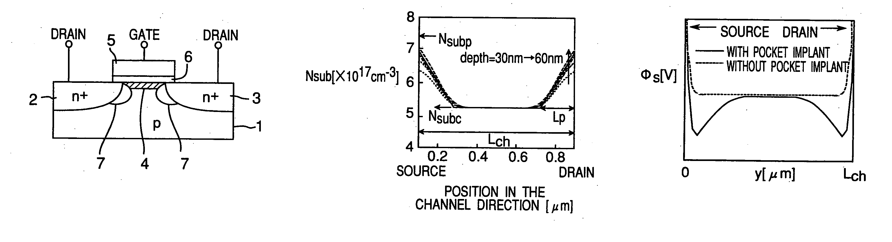
[0032]FIG. 1 shows a construction of pocket implant n-MOSFET. MOSFET has source 2, drain 3, channel 4 formed between source 2 and drain 3, gate electrode 5 which controls channel 4, and gate oxide film 6 formed between channel 4 and gate electrode 5, that are respectively formed on the substrate 1. MOSFET has pocket implant areas 7 formed below channel 4 by implanting impurities of the same type implanted to the source 2 and drain 3 obliquely from the source 2 side and the drain 3 side of the gate electrode 5.

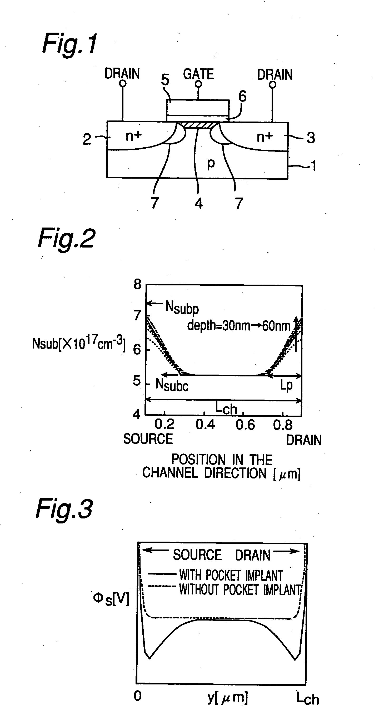
[0033] As shown with the solid line of FIG. 2, the impurity concentration profile below channel 4 of the pocket implant MOSFET is linearly approximated and designated as the threshold voltage model. In FIG. 2, Lch denotes the channel length, Lp the penetration length of pocket implant area 7 in the channel direction, Nsubc the impurity concentration of t...


PUM


Abstract

A threshold voltage model with an impurity concentration profile in a channel direction taken into account is provided in the pocket implant MOSFET. With penetration length of the implanted pocket in the channel direction and the maximum impurity concentration of the implant pocket used as physical parameters, the threshold voltage model is obtained by linearly approximating the profile in the channel direction. By analytically solving the model by using a new threshold condition with inhomogeneous profile taken into account, the threshold voltage can be accurately obtained. Based on thus obtained model, the threshold voltage can be predicted and can be used for circuit design.

Description

[0001] This application is a Divisional of co-pending application Ser. No. 10 / 231,117, filed on Aug. 30, 2002, and claims priority under 35 U.S.C. §120 based thereon. This application also claims priority under 35 U.S.C. §119 based on JP 2001-263752 filed on Aug. 31, 2002. The entire contents of both applications are hereby incorporated by reference.BACKGROUND OF THE INVENTION [0002] 1. Field of the Invention [0003] The present invention relates to a threshold voltage model of pocket implant MOSFET and applications thereof. [0004] 2. Description of the Prior Art [0005] It is essential to effectively suppress short-channel effect in order to miniaturize Metal Oxide Semiconductor Field-Effect Transistor (herein referred to as “MOSFET” for both n-channel and p-channnel), and therefore, the pocket implant technology is popularly used. This pocket implant generates concentration profile with a peak located at a place deep below a source end and a drain end of a channel by implanting impu...

Claims


Application Information

Patent Timeline
Patent Type & Authority Applications(United States)
IPC IPC(8): H01L29/00G06F17/50H01L21/336H01L21/66H01L29/78
CPCG06F2217/78G06F17/5018G06F30/23G06F2119/06H01L22/00
Inventor KITAMARU, DAISUKEMIURA, MICHIKO
Owner SEMICON TECH ACADEMIC RES CENT
Why Eureka
Try Eureka