Electrostatic capacitance sensing device and method of driving the same

Active Publication Date: 2005-04-28
138 EAST LCD ADVANCEMENTS LTD
View PDF5 Cites 14 Cited by
  • Summary
  • Abstract
  • Description
  • Claims
  • Application Information

AI Technical Summary

Benefits of technology

[0013] According to exemplary embodiments of the present invention, thin-film semiconductor devices can constitute an electrostatic capacitance sensing element with high sensitivity. In related art electrostatic capacitance sensing devices, the size thereof is at most approximately several millimeters by several millimeters on a plastic substrate due to using a single-crystal silicon wafer. Exemplary embodiments of the present invention, however, can provide an electrostatic capacitance sensing device having an area some 100 times larger than the related art devices, on a plastic substrate, and moreover, is capable of extremely high-accuracy sen

Problems solved by technology

Hence, they are fragile and subject to breaking when too much finger pressure is applied if they are used as a fingerprint sensor.
In other words, the related art electrostatic capacitance sensing devices are not only expensive, they create huge waste and expense.
Moreover, in a related art electrostatic capacitance sensing device, the sensing sensitivity is poor since an extremely small charge Q needs

Method used


Image

  • Electrostatic capacitance sensing device and method of driving the same
  • Electrostatic capacitance sensing device and method of driving the same
  • Electrostatic capacitance sensing device and method of driving the same

Examples


Embodiment Construction

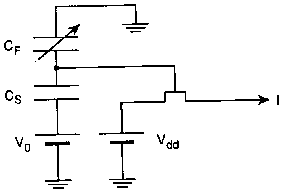
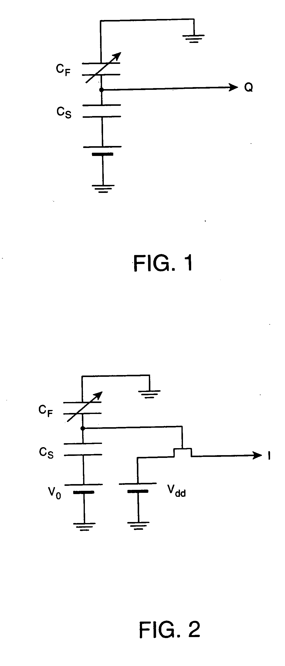
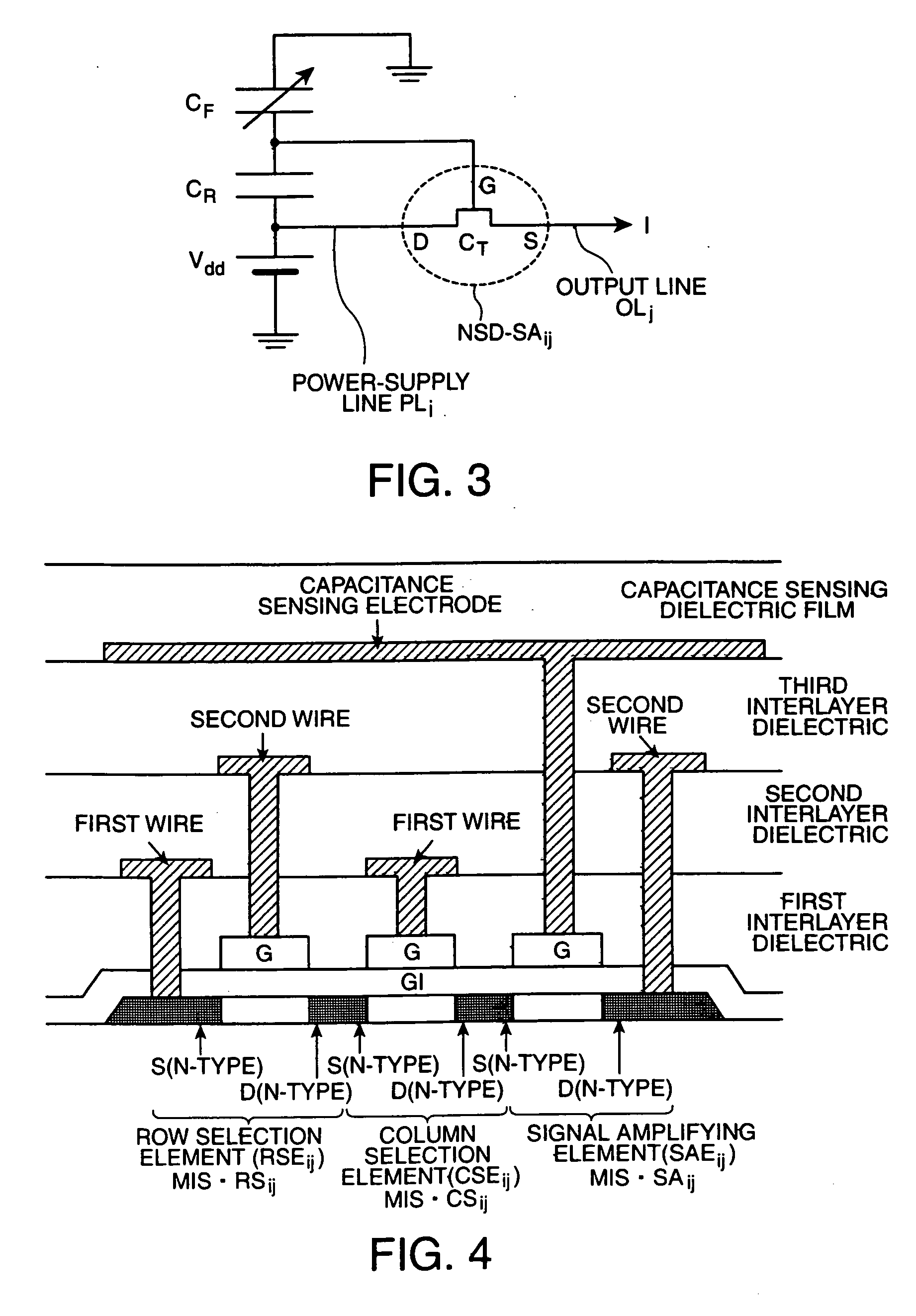
[0024] In exemplary embodiments of the present invention, MIS type thin-film semiconductor devices include metal-insulator-semiconductor films consitutute an electrostatic capacitance sensing device that reads the surface contours of a target object by sensing electrostatic capacitance, which changes according to the distance from a target object. Thin-film semiconductor devices are inexpensively fabricated as large sized semiconductor integrated circuits due to being formed on inexpensive glass substrates, and for example, used as liquid crystal display devices. Therefore, fabricating an electrostatic capacitance sensing device applied to a fingerprint sensor and so forth with thin-film semiconductor devices obviates the need to use an expensive substrate such as a single-crystal silicon wafer, whose production consumes tremendous energy. Instead, the device can be fabricated inexpensively on glass without wasting precious global resources. In addition, a semiconductor integrated c...


PUM


Abstract

An electrostatic capacitance sensing device of exemplary embodiments of the present invention include M number of row lines, N number of column lines that are arranged in a matrix of M rows and N columns, N number of path gates for output signal, and electrostatic capacitance sensing elements provided at the intersections between the row and column lines. The electrostatic capacitance sensing element includes a signal sensing element, a signal amplifying element, a column selection element, and a row selection element. The signal sensing element includes a capacitance sensing electrode and a capacitance sensing dielectric film. The path gate for output signal, the signal amplifying element, the column selection element, and the row selection element are made up of thin-film semiconductor devices.

Description

BACKGROUND OF THE INVENTION [0001] 1. Field of Invention [0002] The present invention relates to an electrostatic capacitance sensing device that reads the surface contours of a fingerprint or other target object having extremely small ridges and valleys, by sensing electrostatic capacitance, which changes according to the distance from the surface of the target object. [0003] 2. Description of Related Art [0004] Japanese Unexamined Patent Publications No. 11-118415, No. 2000-346608, No. 2001-56204, No. 2001-133213 disclose that related art electrostatic capacitance sensing devices, that are used in fingerprint sensors and so forth, a sensor electrode and a dielectric deposited on the sensor electrode, can be formed on a single-crystal silicon wafer. The principle of operation of a related art electrostatic capacitance sensing device is shown in FIG. 1. One of a pair of electrodes in a capacitor is a sensor electrode, and the other is grounded to a human. Furthermore, a dielectric i...

Claims


Application Information

Patent Timeline
IPC IPC(8): A61B5/107G01B7/28A61B5/117G01D5/24G06K9/00
CPCA61B5/1077G06K9/0002G01D5/2405A61B5/1172G06V40/1306
Inventor SANO, JUNICHIMIYASAKA, MITSUTOSHI
Owner 138 EAST LCD ADVANCEMENTS LTD
Why Eureka
Try Eureka