Waveguide system, a device for displaying an image using such a system and a method for displaying an image

a waveguide system and waveguide technology, applied in the field of waveguide systems, can solve the problems of inefficiency, high power consumption, and difficulty in realizing mobile projectors operated by batteries, and achieve the effects of reducing power consumption and space required for light sources, reducing the volume of the device which generates two-dimensional images, and high light transmission efficiency

Inactive Publication Date: 2005-04-28
SONY CORP
View PDF12 Cites 13 Cited by
  • Summary
  • Abstract
  • Description
  • Claims
  • Application Information

AI Technical Summary

Benefits of technology

[0016] The devices and systems in a preferred embodiment of the present invention are advantageous as they have an exceedingly high light transmission efficiency because there is no component which absorbs a significant amount of light. Therefore the devices and systems do not require large light sources to operate, thereby reducing power consumption and the space required for the light sources. As the elements may be integrated on one chip, the volume of the device which generates a two-dimensional image can be made small. These factors make a projector apparatus using the systems and devices according to the invention compact. In this manner, the devices and systems enable a projector apparatus to be extremely small and have a much reduced power consumption in comparison with conventional projectors. The present invention thereby helps to realize mobile image projectors operated by batteries.

Problems solved by technology

This inefficiency requires a brighter light source requiring higher power consumption and a larger size.
This is one of the major reasons why it is difficult to realize mobile projectors which are operated by batteries.

Method used


Image

  • Waveguide system, a device for displaying an image using such a system and a method for displaying an image
  • Waveguide system, a device for displaying an image using such a system and a method for displaying an image
  • Waveguide system, a device for displaying an image using such a system and a method for displaying an image

Examples


Embodiment Construction

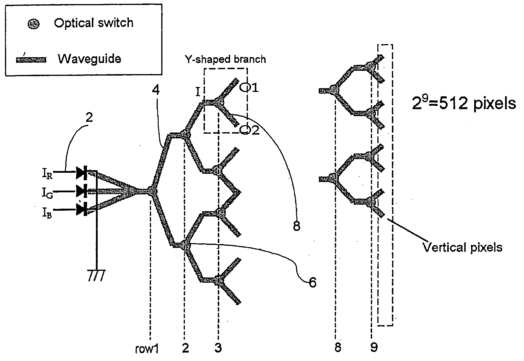
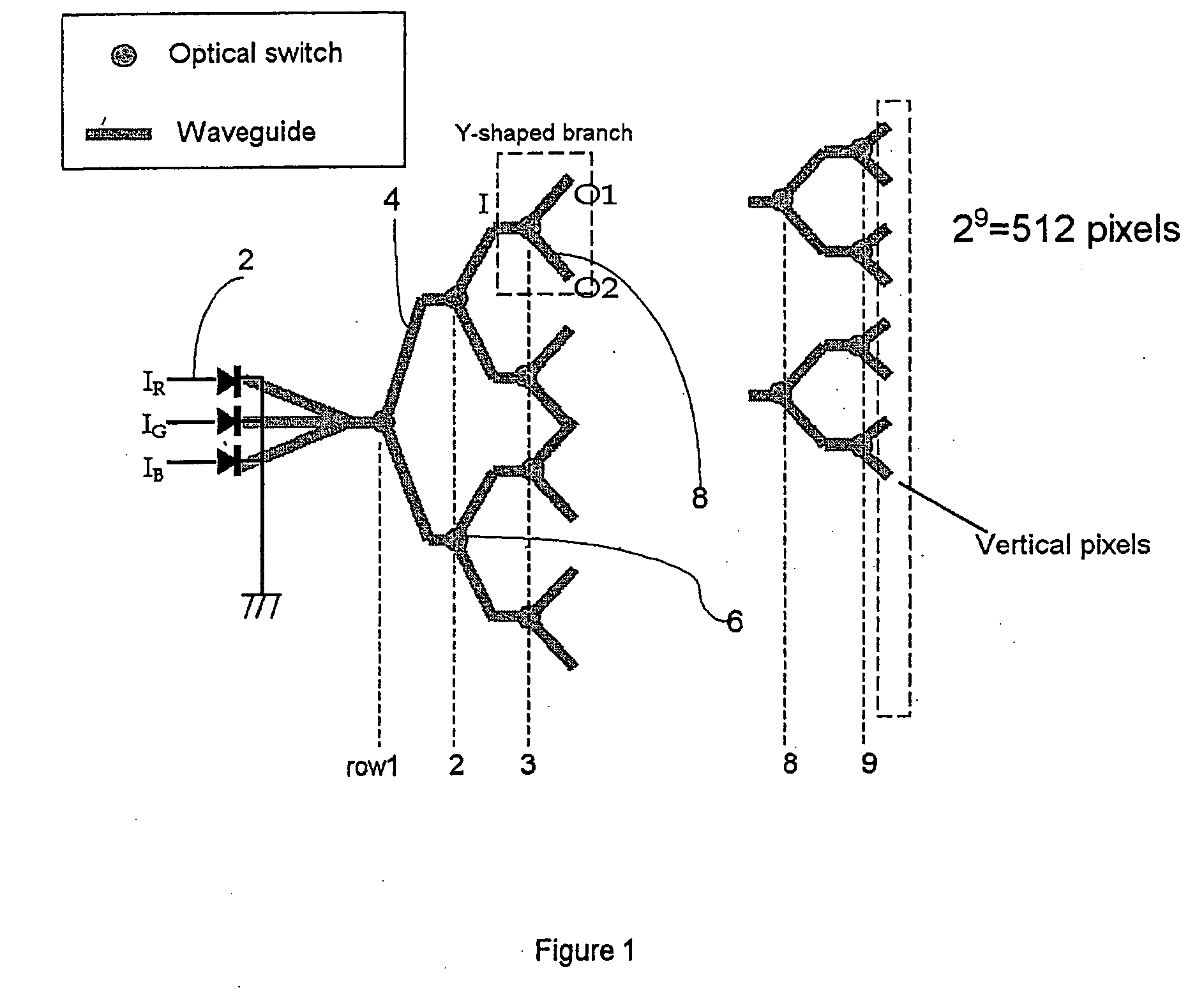
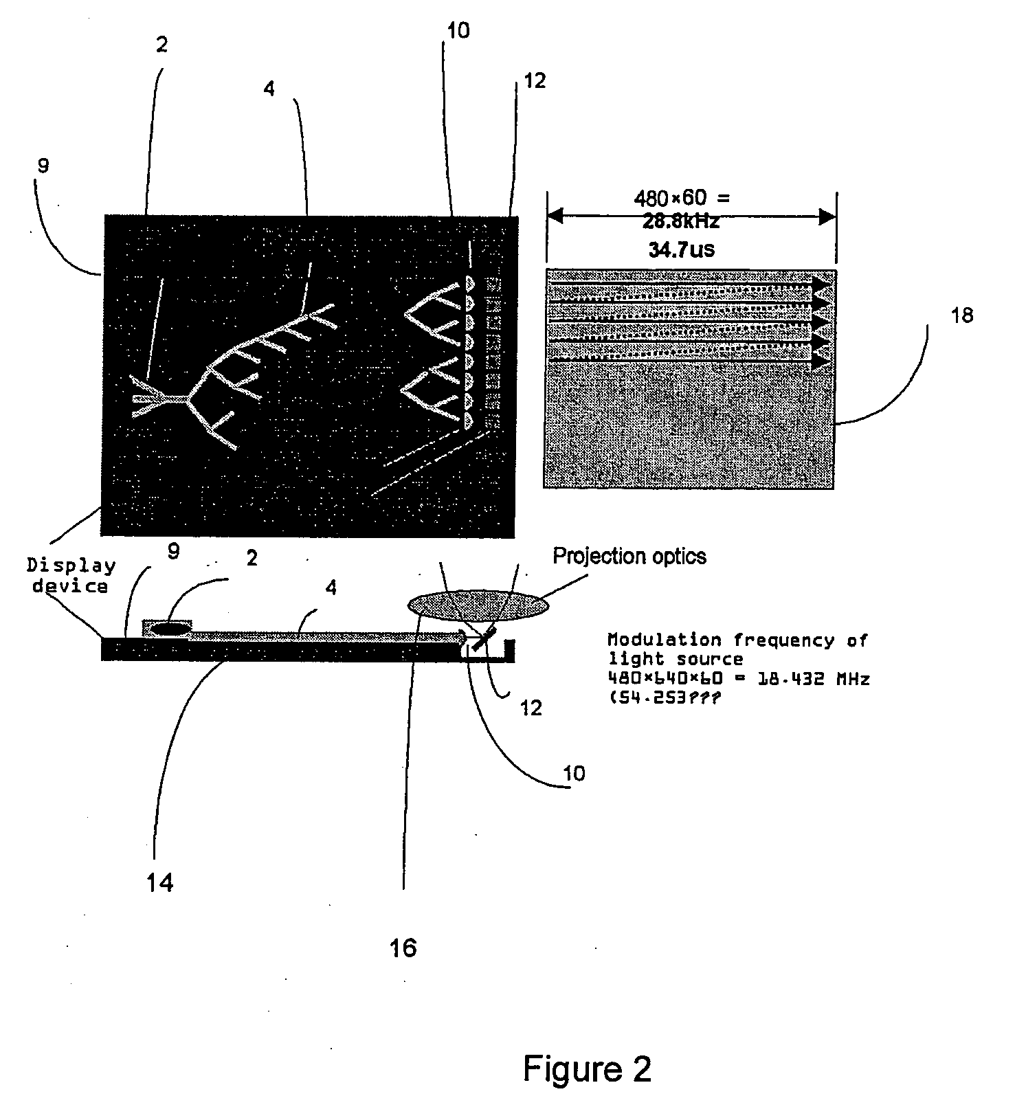
[0024]FIG. 1 shows a schematic of a display device embodying the invention comprising an arrangement of light sources 2, waveguides 4, and optical switches 6. The light sources 2 feed light into the waveguides 4 and light is propagated through the waveguides which are connected to the plurality of optical switches 6. The optical switches 6 switch the light received into one of two outlets according to control signals received from control circuits (not shown). The outputs of the switches 6 are each connected to the inputs of a further row of optical switches which, in turn, are cascaded to, for example, nine rows of switches, resulting in 512 output waveguides. Thus, the light fed to the input of the first waveguide may be switched to any one of the 512 output waveguides. This is explained in more detail below.

[0025] Light Emitting Diodes (LEDs) or Laser Diodes (LDs) are suitable for the light sources 2. For colour images, red, green and blue LEDs or LDs are required. The intensity...


PUM

PropertyMeasurementUnit
light transmittanceaaaaaaaaaa
total light transmittanceaaaaaaaaaa

Abstract

A device such as an integrated display device and projector apparatus using said display device for projecting an image on a screen comprises a number of light sources, waveguides, optical switches, micro-lenses and scanning mirrors. The display apparatus consists of said display device, a modulator circuit, an optical switch controller, a scanning mirror controller, a synchronizer and projection optics. This device enables the projector apparatus to be extremely small and to reduce its power consumption in comparison with conventional projectors.

Description

FIELD OF THE INVENTION [0001] The present invention relates to a waveguide system, a device for displaying an image using such a system and a method for displaying an image. In particular, the present invention relates to information display devices, especially to projection display devices. BACKGROUND OF THE INVENTION [0002] Liquid crystal display (LCD) panels are utilized for most conventional projectors. A typical LCD panel consists of two sheets of polarizer, a liquid crystal cell, thin film transistors (TFT) and colour filters. The light transmittances of these components are approximately 50% for a pair of polarizer sheets, 80% for an aperture of TFT and 30% for colour filters, respectively. Therefore, the total light transmittance of all components is approximately 12%. This means that only 12% of the light from a projection light source can be transmitted through the LCD panel. This inefficiency requires a brighter light source requiring higher power consumption and a larger...

Claims


Application Information

Patent Timeline
Patent Type & Authority Applications(United States)
IPC IPC(8): G02B6/42G02B6/122G02B6/28G02B26/10G02B27/18G02F1/065G02F1/13G02F1/1333G02F1/141G02F1/313G09G3/00
CPCG02B6/2804G09G3/002G02F1/3137G02F1/1326
Inventor ISHIDA, TAKEHISA
Owner SONY CORP
Why Eureka
Try Eureka