Manufacturing method of semiconductor integrated circuit device

a manufacturing method and integrated circuit technology, applied in the direction of instruments, photomechanical equipment, originals for photomechanical treatment, etc., can solve problems such as attenuation of exposure beams, and achieve the effect of reducing pattern data

Inactive Publication Date: 2005-04-28
HITACHI LTD
View PDF2 Cites 226 Cited by
  • Summary
  • Abstract
  • Description
  • Claims
  • Application Information

AI Technical Summary

Benefits of technology

[0008] Under such circumstances, it is an object of the present invention to provide a technique that is capable of reducing pattern data when designing each phase shift mask.
[0013] The present invention requires no auxiliary pattern for any light transmission pattern in each sparse region, so that pattern data can be reduced when designing each phase shift mask.

Problems solved by technology

The official gazette of JP-A No. 83032 / 1994 describes a problem that arises when an electron beam drawing resist or silicon dioxide is used for a phase shift material of the phase shift masks.
The problem is attenuation of an exposure beam caused by the transmission factor of the subject phase shifter.
However, in the case of a technique that prepares an auxiliary pattern for each solitary pattern in a phase shift mask having both a massed region to which massed patterns are to be transferred and a sparse region to which a solitary pattern is to be transferred, the present inventor et al have found that the following problems arise from the use of the technique.
These become problems in the practical use of the technique.

Method used


Image

  • Manufacturing method of semiconductor integrated circuit device
  • Manufacturing method of semiconductor integrated circuit device
  • Manufacturing method of semiconductor integrated circuit device

Examples


first embodiment

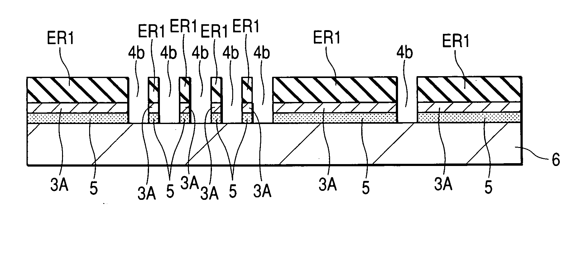
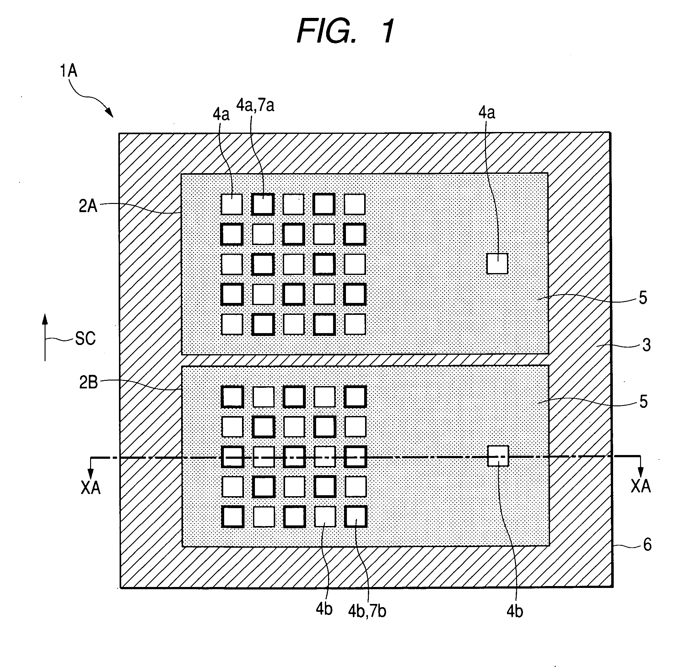
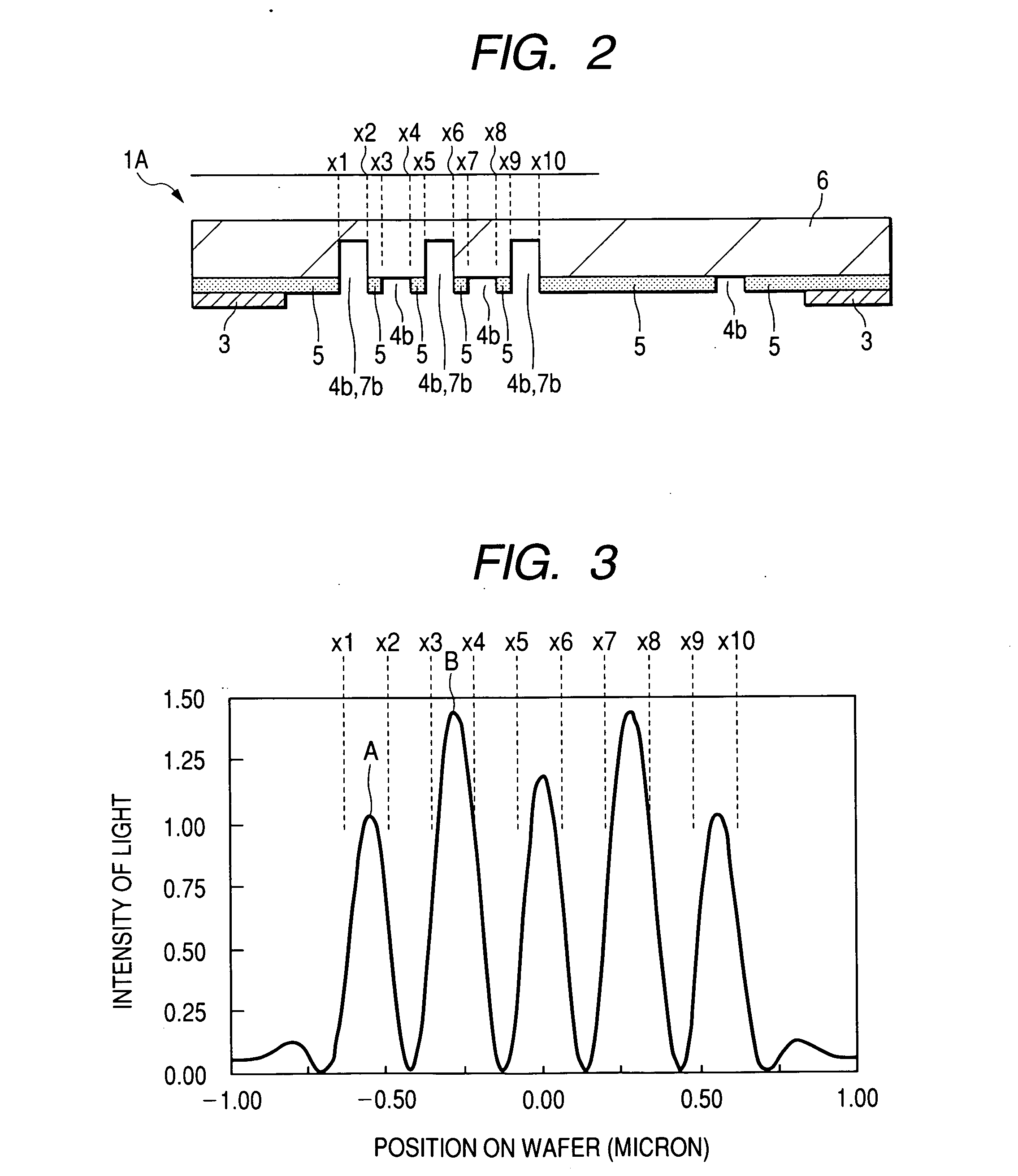
[0054]FIGS. 1 and 2 show an example of a mask employed for a method of manufacture of a semiconductor integrated circuit device according to a first embodiment of the present invention. FIG. 1 shows an overall top view of the mask 1A of this first embodiment of the present invention. FIG. 2 shows a cross sectional view of the mask 1A as seen along line XA-XA in FIG. 1. The top view of the mask 1A shown in FIG. 1 is hatched specially to make it easier to understand the description. And, coordinates x1 to x10 are given to describe areas of the mask 1A in detail.

[0055] The mask 1A in this first embodiment is used to transfer hole patterns (contact holes or through-holes) as integrated circuit patterns. On a main surface of this mask 1A, there are disposed, for example, two transfer areas 2A and 2B in the vertical direction (the scanning direction SC of an exposure apparatus) as seen in FIG. 1 so as to be limited by a shielding pattern 3. Each of the transfer areas 2A and 2B is equival...

second embodiment

[0084] In this second embodiment, the present invention is applied to a mask for transferring line patterns (gate electrodes or wirings) as integrated circuit patterns. FIG. 21 shows a top view of a mask 1B according to this second embodiment. FIG. 22 shows a cross sectional view of the mask 1B as seen along line XB-XB in FIG. 21. In each transfer area 2A / 2B, there are flat band-like light transmission patterns 4c / 4d used for transferring line patterns. In the massed region of each transfer area 2A / 2B, a plurality of light transmission patterns 4c / 4d are disposed side by side in the horizontal direction as seen in FIG. 21. In the massed region of each transfer area 2A / 23, a phase shifter 7a / 7b is disposed in every second one of the plurality of light transmission patterns 4c / 4d. However, also in this second embodiment, phase shifters 7a and 7b are disposed symmetrically and are inverted in phase in the transfer areas 2A and 2B, just like in the first embodiment. In the sparse region...

third embodiment

[0087] In this third embodiment, a description will be given of a method for forming phase shifters with a film (phase shift film stacking method or stacking phase shifter).

[0088]FIGS. 23 and 24 show cross sectional views of the major portions at each of which the transfer areas 2A and 23 of the mask 1C in this third embodiment are overlaid one upon another for overlay exposure. FIG. 24 shows a cross sectional view of a portion at a line equivalent to the line XA-XA in FIG. 1, while FIG. 23 shows a cross sectional view of a portion to be overlaid upon the other portion shown in FIG. 24. The cross sectional view is for a portion at a line in parallel to the line XA-XA in the transfer area 2A in FIG. 1.

[0089] In the mask 1C in this third embodiment, the phase shifters 7c and 7d are made of, for example, a resist film or a SOG (Spin On Glass) film. The top surface shape of the mask 1C is similar to any of those shown in FIGS. 1 and 21. If phase shifters are made of a film, the thickn...


PUM

PropertyMeasurementUnit
lengthaaaaaaaaaa
lengthaaaaaaaaaa
lengthaaaaaaaaaa

Abstract

In a massed region of each of a plurality of transfer areas of a mask a plurality of light transmission patterns are formed by opening a half-tone film. A phase shifter is disposed in each of the light transmission patterns so that a 180° phase inversion occurs between the lights that transmit through adjacent light transmission patterns. In a sparse region of the plurality of transfer areas a solitary light transmission pattern is formed by opening the half-tone film. Both shape and size are the same among the light transmission patterns, which are disposed symmetrically in both the massed and sparse regions about the center between the transfer areas. The phase shifters in the massed regions are disposed so that the phase of each phase shifter in one of the transfer areas comes to be opposed to that of its counterpart in the other transfer area. In the exposure process, those transfer areas are overlaid one upon another in the same chip region.

Description

CLAIM OF PRIORITY [0001] The present invention claims priority from Japanese application JP 2003-363005, filed on Oct. 23, 2003, the content of which is hereby incorporated by reference into this application. BACKGROUND OF THE INVENTION [0002] The present invention relates to a technique for manufacturing a semiconductor integrated circuit device, and, more particularly, to a technique for exposing objects using a phase shift mask. [0003] In the case of the next generation 65 nm node lithography, there is a demand for use of the ArF scanner which has been employed for the 90 nm node lithography. However, because the wiring length of the logic LSI for the 90 nm node lithography is about 100 to 120 nm and the K1 factor of R=K1×λ / NA for denoting resolution R is about 0.5, the requirement for the 90 nm node lithography can be satisfied using a weak super resolution technique, while a strong super resolution technique is indispensable to satisfy the requirements for the 65 nm node lithog...

Claims


Application Information

Patent Timeline
Patent Type & Authority Applications(United States)
IPC IPC(8): G03C5/00G03F1/30G03F1/32G03F1/68G03F7/20H01L21/027H01L21/302H01L21/311H01L21/768
CPCG03F1/0061G03F1/14H01L21/76808G03F1/32H01L21/31144G03F1/30G03F1/50
Inventor HASEGAWA, NORIOHAYANO, KATSUYAHOTTA, SHOJI
Owner HITACHI LTD
Why Eureka
Try Eureka