Scan test method, device, and system

Inactive Publication Date: 2005-04-28
SAMSUNG ELECTRONICS CO LTD
View PDF7 Cites 23 Cited by
  • Summary
  • Abstract
  • Description
  • Claims
  • Application Information

AI Technical Summary

Benefits of technology

[0042] Exemplary embodiments of the present invention provide a scan test method, device, and system which may reduce the overhead of a semiconductor chip by sharing scan cells connected to input / output ports of an embedded memory, and may detect faults in a plurality of embedded memories.

Problems solved by technology

A sequential logic circuit for example, a flip-flop, controlling an internal node may be more difficult, due to a clock difference of one cycle that may be generated between a front terminal node and a rear terminal node.
That is, it may be difficult to input an appropriate value to the input pin in view of the above cycle.
Accordingly, it may more difficult to detect a fault in semiconductor chips which may have many flip-flops.
However, the embedded memory may not perform fault detection because a conventional scan cell of FIG. 2A because data may be delayed by one cycle due to the flip-flop of the scan cell in the capture mode.
The fault may not be detected at all input ports and / or output ports of the embedded memory 30, which may cause the fault coverage to deteriorate in the semiconductor chip 1.
Scan cells may be added to improve the fault coverage of the embedded memory and may result in an increase in the overhead of the entire semiconductor chip.
The overhead may further increase as the embedded memories increase in number according to a high-density integration of a semiconductor chip.
However, the scan cell which may used to test and the logic circuit which may be used for the normal operation may have very large area ratio.
Specifically, many embedded memories may be additionally installed and the ratio of the area (wrapper) to the area (normal function) may be 10% or greater, thereby causing more larger overhead in which the total area of the semiconductor chip may be increased due to the scan cell.

Method used


Image

  • Scan test method, device, and system
  • Scan test method, device, and system
  • Scan test method, device, and system

Examples


Embodiment Construction

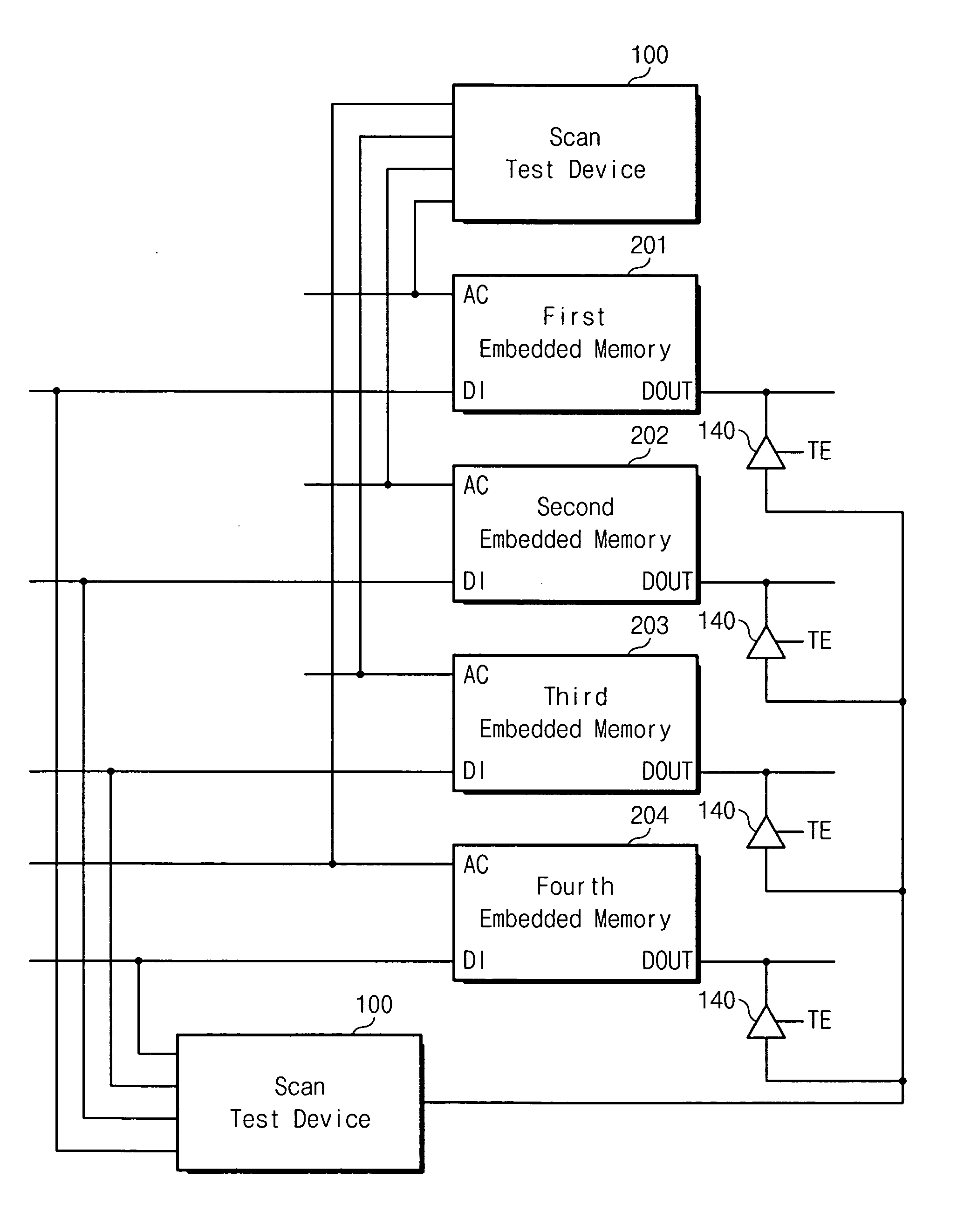
[0069]FIG. 6 is a circuit diagram illustrating a scan test device according to exemplary embodiments of the present invention. The scan test device 100 may detect faults in embedded memories which may have the same, or substantially the same, construction and / or embedded memories which may have different constructions.

[0070] The scan test device 100 may include a first select unit 110 which may selectively output data inputs (in_k; k=1 to n), which may detect faults in the embedded memories, in response to a select signal S; a second select unit 120 which may selectively output a data input from the first select unit 110 and / or a scan input from an input terminal, in response to a scan enable signal SE; and a flip-flop 130 which may output data from the second select unit 120 to an output terminal in response to a clock signal CK. The scan test device 100 may also include a third select unit which may perform a normal operation and / or a test operation in response to a test enable s...


PUM


Abstract

A scan test method, device, and system may be provided to detect faults in embedded memories. The device may include a first select unit which may selectively output data inputs and may detect the faults in the embedded memories in response to a select signal S, a second select unit which may selectively output a data input from the first select unit and / or a scan input from an input terminal in response to a scan enable signal SE, and a flip-flop which may output data output from the second select unit to an output terminal in response to a clock signal CK.

Description

CROSS-REFERENCE TO RELATED APPLICATIONS [0001] This U.S. nonprovisional patent application claims priority under 35 U.S.C. § 119 of Korean Patent Application 2003-74686 filed on Oct. 24, 2003, the entire contents of which are hereby incorporated by reference. BACKGROUND OF THE INVENTION [0002] The present invention may relate to a scan test method, device, and system, and more particularly, to a scan test method, device, and system for reducing an overhead of a semiconductor chip. [0003] Fault coverage may correspond to a ratio of the number of detected faults to the total number of generated faults (defects), for example, 95% of the fault coverage may indicate that 95% of faults in a semiconductor chip may be detected. [0004] Test coverage of a semiconductor chip may enable the recognition of where a fault may have been generated in the semiconductor chip, and may take an appropriate action for the generated fault. [0005]FIG. 1A illustrates an example of fault detection. A semicond...

Claims


Application Information

Patent Timeline
IPC IPC(8): G01R31/3185G06F11/22G01R31/28G11C29/00G11C29/48H01L21/822H01L27/04H03K19/00
CPCG01R31/318536G11C2029/3202G11C2029/0401G11C29/48G11C29/00
Inventor LEE, HOI-JIN
Owner SAMSUNG ELECTRONICS CO LTD
Why Eureka
Try Eureka