Field effect transistor and manufacturing method thereof

a field effect transistor and manufacturing method technology, applied in the direction of semiconductor devices, transistors, electrical devices, etc., can solve the problems of large leak current, large leak current, and serious problem of shallow junction formation

Inactive Publication Date: 2005-05-05
KK TOSHIBA
View PDF6 Cites 87 Cited by
  • Summary
  • Abstract
  • Description
  • Claims
  • Application Information

AI Technical Summary

Benefits of technology

[0011] A field effect transistor according to an aspect of the invention comprises a first semiconductor region forming a channel region, a gate electrode insulatively disposed above the first semiconductor region, a source electrode and a drain electrode which are formed, respectively, on both sides of the first semiconductor region in a position corresponding to the gate electrode, and second semiconductor re

Problems solved by technology

However, the limitation of miniaturization in future is pointed out and formation of shallow junction becomes a serious problem.
However, since the field effect transistor utilizes the Schottky junction, there occurs a problem that a leak current becomes large.
However, in this type of Schottky 0transistor, there occurs a pr

Method used


Image

  • Field effect transistor and manufacturing method thereof
  • Field effect transistor and manufacturing method thereof
  • Field effect transistor and manufacturing method thereof

Examples


first embodiment

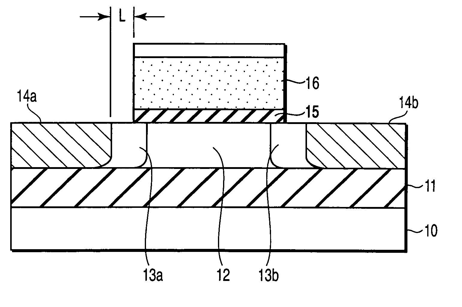
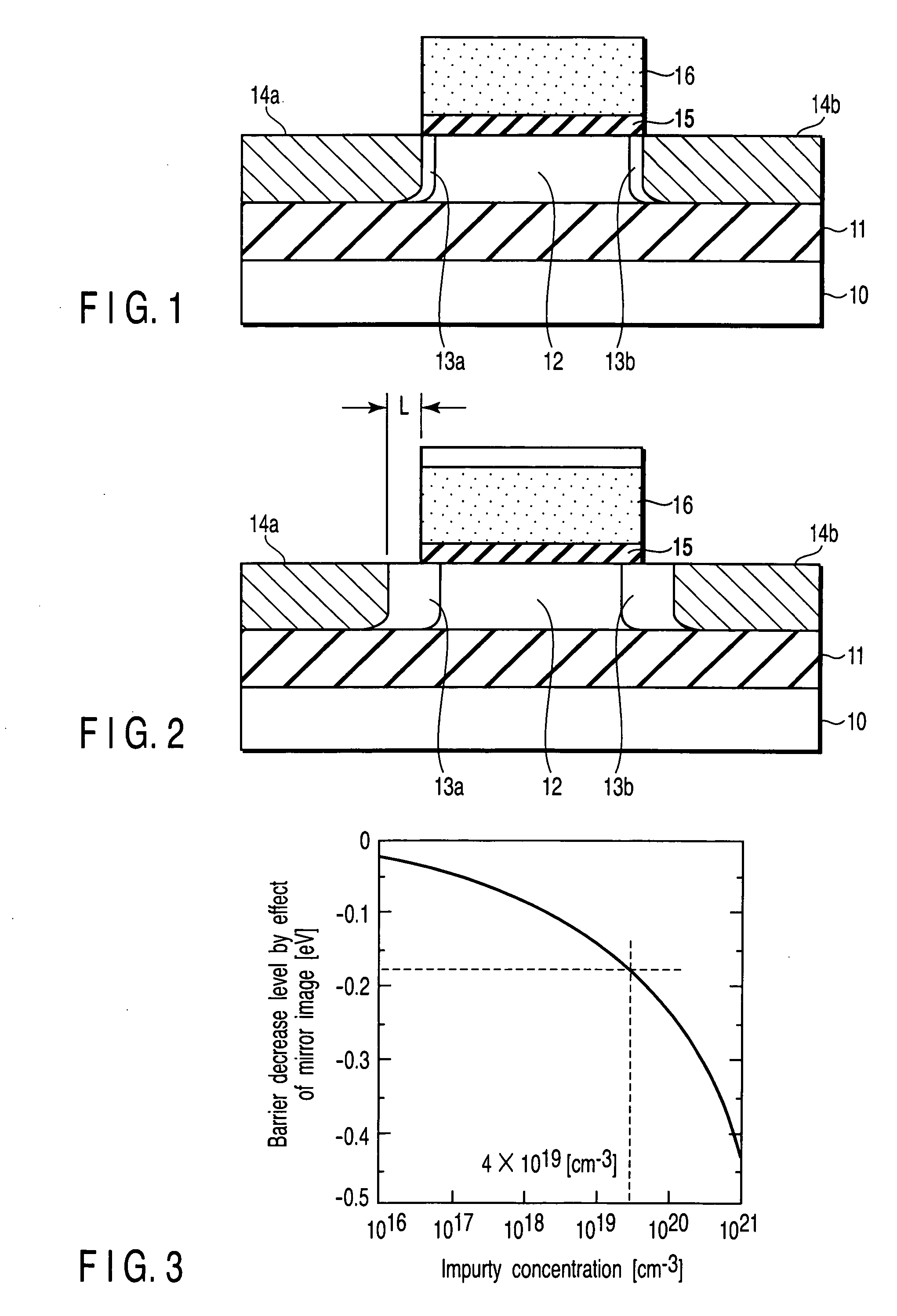
[0043]FIG. 1 is a cross sectional view showing the element structure of a MIS field effect transistor according to a first embodiment of this invention.

[0044] A buried insulating film 11 formed of a silicon oxide film is formed on a silicon substrate 10 and first and second semiconductor regions 12, 13 (13a, 13b) and metal source and drain electrodes 14 (14a, 14b) are formed on the buried insulating film 11. A gate electrode 16 is formed above the semiconductor regions 12, 13 with a gate insulating film 15 disposed therebetween.

[0045] The first semiconductor region 12 is formed of a p-type layer having boron (B) doped therein, for example, to form a channel region. The second semiconductor regions 13 are each formed of an n+-type layer having As doped therein with high impurity concentration, for example, and formed with extremely thin width to sandwich the first semiconductor region 12 in the channel lengthwise direction. The source and drain electrodes 14 are formed of metal or ...

second embodiment

[0072]FIGS. 9A to 9F are cross sectional views showing the manufacturing steps for forming a MIS field effect transistor according to a second embodiment of this invention. In this embodiment, a case wherein the transistor is formed on an Si substrate instead of the SOI substrate is shown.

[0073] First, as shown in FIG. 9A, a silicon substrate 20 (which is hereinafter simply referred to as a substrate) having the plane orientation (100) and specific resistance 2 to 6 Ωcm is prepared. Then, an isolation region (not shown) is formed by use of a known method and a p-type impurity region (first semiconductor region) 22 which is used as a channel is formed by use of an ion-implantation method or the like.

[0074] Next, as shown in FIG. 9B, a silicon oxide film with a film thickness of 1 to 10 nm is formed on the surface of the first semiconductor region 22 by use of an oxide film forming method (which is hereinafter referred to as an oxide film forming method) as will described later. The...

third embodiment

[0086]FIG. 10 is a cross sectional view showing the element structure of a MIS field effect transistor according to a third embodiment of this invention.

[0087] The present embodiment can be attained by using an SOI substrate which is the same as that of the first embodiment in the second embodiment. That is, a buried insulating film 31 such as a silicon oxide film is formed on a silicon substrate 30. Then, a first semiconductor region 32, second semiconductor region 33, source and drain regions 34, gate insulating film 35, side wall insulating films 37, HALO regions 38 and high-concentration impurity layer 39 are formed on the structure.

[0088] Thus, the present embodiment has basically the same configuration as that of the second embodiment except that the SOI substrate is used and the manufacturing method thereof is basically the same as that of the second embodiment. Therefore, the same effect as that of the second embodiment can be attained.


PUM


Abstract

A field effect transistor includes a first semiconductor region forming a channel region, a gate electrode insulatively disposed above the first semiconductor region, source and drain electrodes formed to sandwich the first semiconductor region in a channel lengthwise direction, and second semiconductor regions formed between the first semiconductor region and the source and drain electrodes and having impurity concentration higher than the first semiconductor region. The thickness of the second semiconductor region in the channel lengthwise direction is set to a value equal to or less than depletion layer width determined by the impurity concentration so that the second semiconductor region is depleted in a no-voltage application state.

Description

CROSS-REFERENCE TO RELATED APPLICATIONS [0001] This application is based upon and claims the benefit of priority from prior Japanese Patent Applications No. 2003-314328, filed Sep. 5, 2003 and No. 2004-251534, filed Aug. 31, 2004, the entire contents of both of which are incorporated herein by reference.BACKGROUND OF THE INVENTION [0002] 1. Field of the Invention [0003] This invention relates to a semiconductor device and more particularly to a MIS field effect transistor having a source and drain improved and a manufacturing method thereof. [0004] 2. Description of the Related Art [0005] In order to enhance the performance of a semiconductor integrated circuit, it is necessary to enhance the performance of field effect transistors which are the constituent elements thereof. The guiding principle for the improvement of the performance of the elements is based on scaling and the element performance has been enhanced by miniaturizing the elements so far. However, the limitation of min...

Claims


Application Information

Patent Timeline
IPC IPC(8): H01L21/336H01L21/28H01L21/77H01L21/8238H01L21/84H01L27/08H01L27/092H01L27/12H01L29/417H01L29/45H01L29/78H01L29/786
CPCH01L21/84H01L27/1203H01L29/458H01L29/6653H01L29/6659H01L29/66643H01L29/78645H01L29/66795H01L29/7833H01L29/7839H01L29/785H01L29/78618H01L29/66772H01L29/66477
Inventor KINOSHITA, ATSUHIROKOGA, JUNJI
Owner KK TOSHIBA
Why Eureka
Try Eureka