Semiconductor integrated circuit testing device and method

Inactive Publication Date: 2005-05-05
CANON KK
View PDF8 Cites 22 Cited by
  • Summary
  • Abstract
  • Description
  • Claims
  • Application Information

AI Technical Summary

Benefits of technology

[0020] In the light of the foregoing, it is an object of the present invention to provide a semiconductor integrated circuit testing device and method which are c

Problems solved by technology

Now, in the conventional testing method based on the test pattern in which the expected value of the output pattern becomes clear, as the scale of a semiconductor integrated circuit to be measured becomes large, it becomes difficult to produce a test pattern in which all logic states are simulated, and hence an area which is undetected with the test pattern exists.
As a result, there is a possibility that the nonconformity may occur such that in a machinery or the like having a semiconductor integrated circuit as one of constituent elements, when the machinery is used in the above-mentioned undetected area, the machinery does not

Method used


Image

  • Semiconductor integrated circuit testing device and method
  • Semiconductor integrated circuit testing device and method
  • Semiconductor integrated circuit testing device and method

Examples


embodiment 1

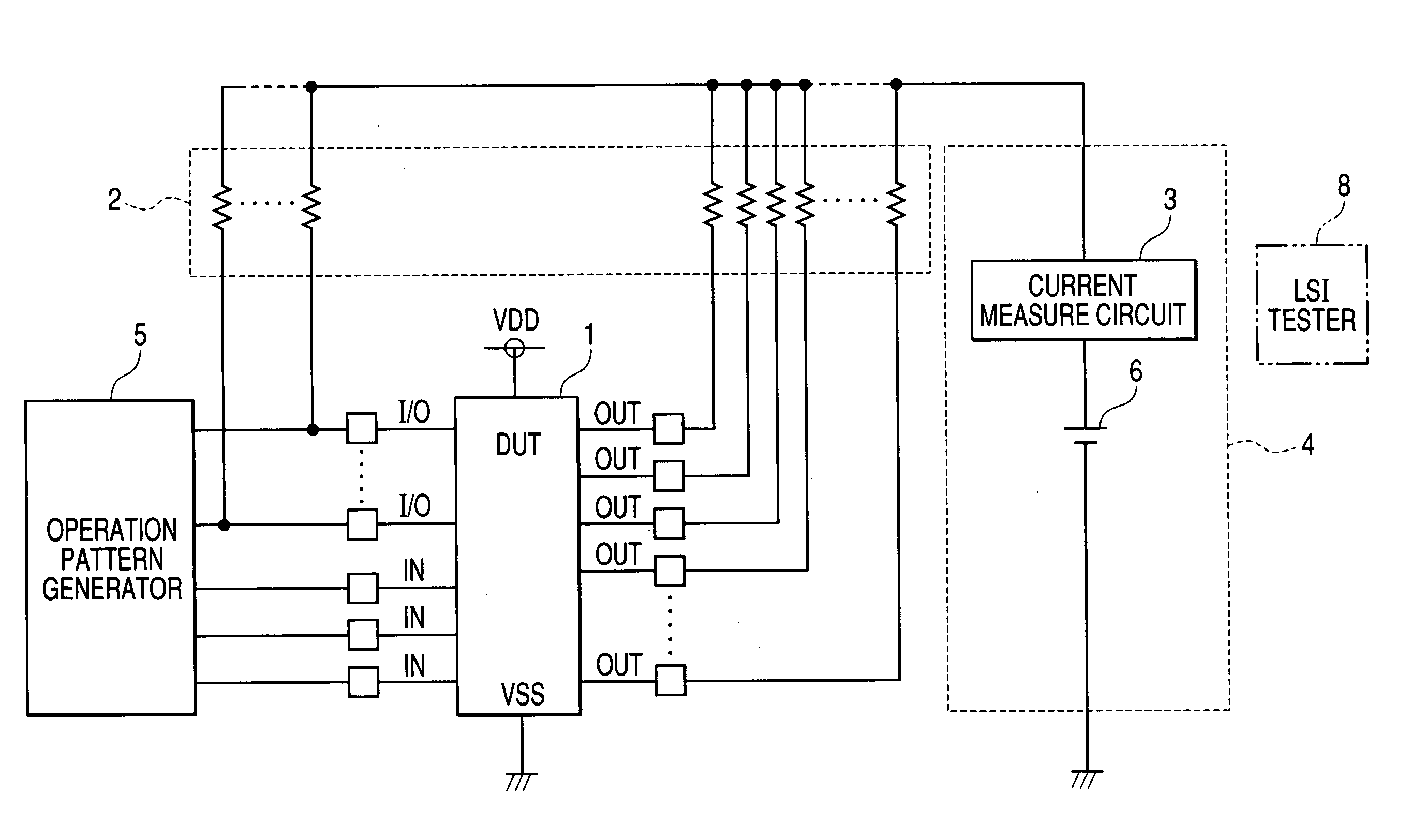
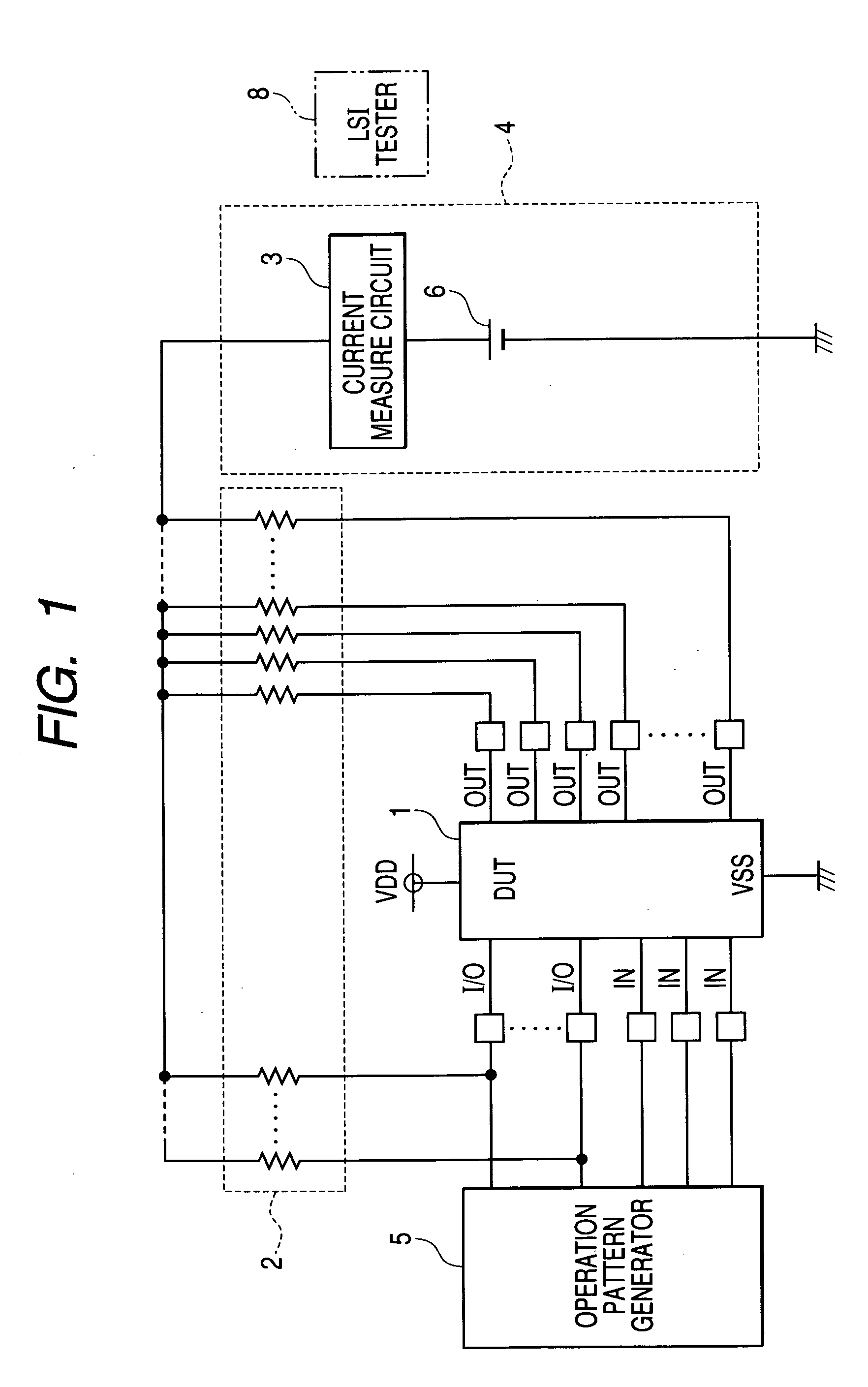
[0049]FIG. 1 is a block diagram, partly in circuit diagram, showing a configuration of a semiconductor integrated circuit testing device according to Embodiment 1 of the present invention.

[0050] Referring to FIG. 1, reference numeral 1 designates a semiconductor integrated circuit (DUT) including a logic circuit becoming an object of a test. Output terminals (OUT) and input-output terminals (I / O) of the DUT 1 are all connected to a voltage application circuit 4 through a resistor unit 2. The resistor unit 2 includes a plurality of resistors which are connected in parallel to one another and which have the same resistance values. One terminals of a plurality of resistors are connected to the output terminals and the input-output terminals of the DUT 1, respectively, and the other terminals thereof are all short-circuited to be connected to the voltage application circuit 4. The voltage application circuit 4 includes a D.C. power supply 6 having a grounded minus terminal, and a curre...

embodiment 2

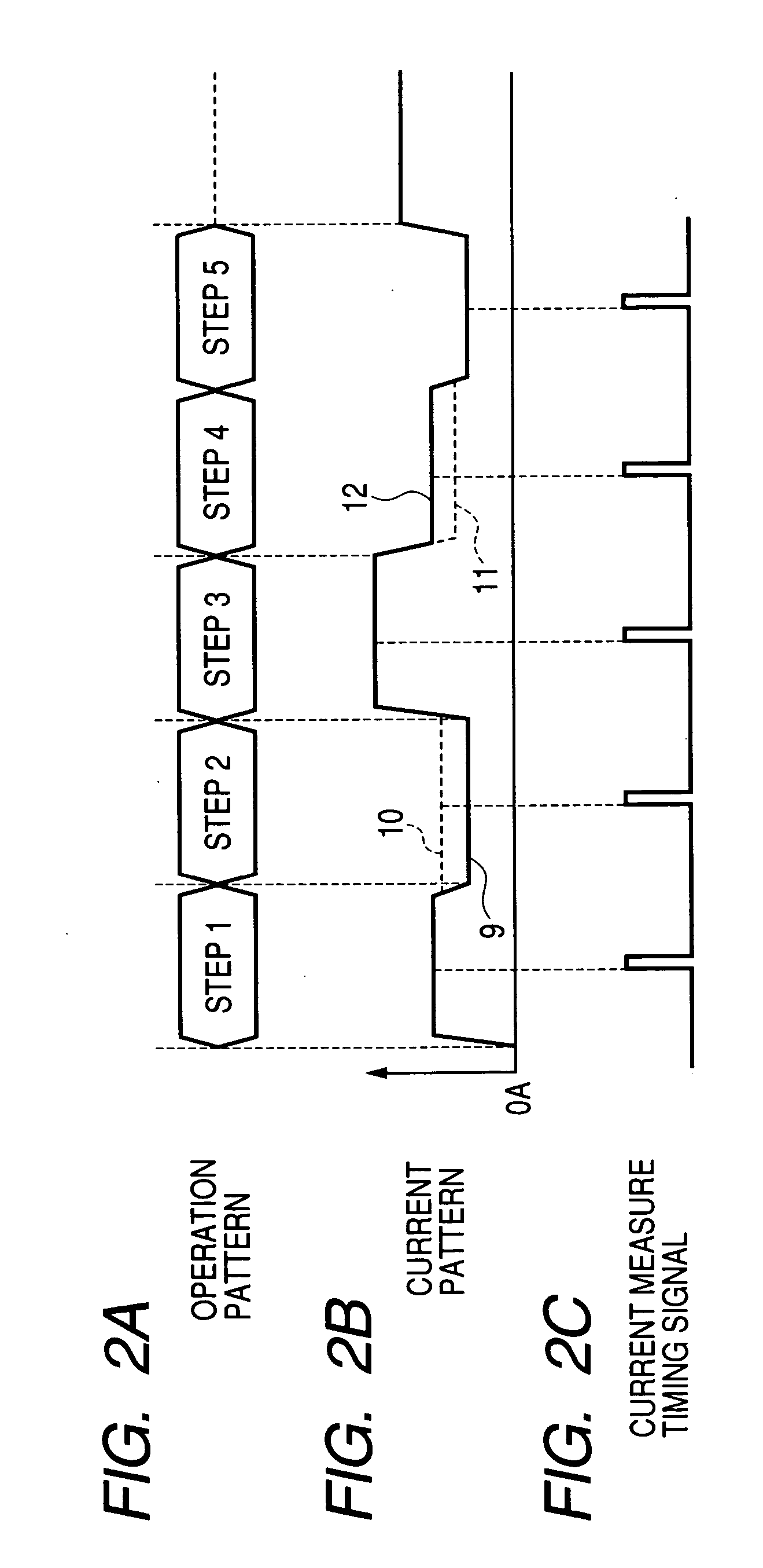
[0062] In Embodiment 1, the pattern signal of the predetermined operation pattern is input to the DUT, and the number of terminals of the DUT at each of which the output logic goes to 0 accordingly is compared with the number of terminals at each of which the output logic goes to 0 in correspondence to the same predetermined operation pattern input to the non-defective sample every operation step of the predetermined operation pattern to judge whether the DUT is a non-defective or a defective.

[0063] In the above-mentioned comparison with respect to the number of terminals, more specifically, a total sum of values of the currents caused to flow through the resistors which are connected to the output terminals and the input-output terminals (in the output state) of the DUT, respectively, in the stationary state for each operation step is compared with a total sum of values of such currents in the non-defective sample, thereby judging whether the DUT is a non-defective or a defective....

embodiment 3

[0084] Next, Embodiment 3 of the present invention will hereinafter be described. Since a configuration of Embodiment 3 is basically the same as that of Embodiment 2, the configuration of Embodiment 2 will be diverted to the description of Embodiment 3.

[0085] In Embodiment 3, the block of the DUT which is judged to be a defective in Step S4 or Step S8 of the flow chart of Embodiment 2 shown in FIG. 4 is further repeatedly divided into blocks to narrow a defective terminal.

[0086]FIG. 5 is a flow chart showing a procedure for narrowing a defective terminal in Embodiment 3.

[0087] Steps S11 to S14 in the flow chart are executed after execution of Step S4 or Step S8 of the flow chart of Embodiment 2 shown in FIG. 4.

[0088] First of all, in Step S11, the block of the DUT which is judged to be defective in Step S4 or Step S8 in Embodiment 2 is further divided into a plurality of blocks.

[0089] In next Step S12, the same current measure and comparison as those in Steps S1 to S9 of Embodi...


PUM


Abstract

A plurality of resistors is connected to a plurality of output terminals of a semiconductor integrated circuit, respectively, and a predetermined voltage is applied to the plurality of resistors. Also, a predetermined operation pattern signal used to test functions of the semiconductor integrated circuit is input to a plurality of input terminals of the semiconductor integrated circuit. Thus, a total sum of amounts of currents caused to flow through the plurality of resistors, respectively, is measured. The total sum of amounts of currents thus measured is compared with a normal value of a total sum of amounts of currents which are measured in a non-defective sample which is used instead of the semiconductor integrated circuit and is verified in advance to normally operate. It is judged based on the comparison results whether or not the semiconductor integrated circuit is normal. As a result, whether or not the semiconductor integrated circuit is a non-defective or a defective can be simply judged without performing logic simulation and failure simulation.

Description

BACKGROUND OF THE INVENTION [0001] 1. Field of the Invention [0002] The present invention relates to a semiconductor integrated circuit testing device and method for testing functions of a semiconductor integrated circuit. [0003] 2. Related Background Art [0004] Heretofore, in testing functions of a semiconductor integrated circuit including a logic circuit, a method has been adopted in which a pattern signal of a predetermined test pattern for testing the functions of the semiconductor integrated circuit is input to the semiconductor integrated circuit, and a signal value of an output pattern from the semiconductor integrated circuit is compared with an output pattern expected value, thereby judging whether the semiconductor integrated circuit is a defective or a non-defective (refer to “VLSI Test / Failure Analysis Technology,” Triceps Co., Ltd., pp. 119 and 120 (1992). The predetermined test pattern is a test pattern set such that an expected value of an output pattern which is to ...

Claims


Application Information

Patent Timeline
IPC IPC(8): G01R31/30G01R31/317
CPCG01R31/31703G01R31/3004G01R31/3193
Inventor WATANABE, HIROSHIIKEDA, TATSUJITAKAHASHI, KAZUYA
Owner CANON KK
Why Eureka
Try Eureka