Power level controlling of first amplification stage for an integrated RF power amplifier

a technology of power amplifier and power amplifier, which is applied in the direction of amplifiers, dc-amplifiers with dc-coupled stages, high-frequency amplifiers, etc., can solve the problems of difficult to predict the amplitude of the output signal with any great accuracy, and the inability to provide the overall pa output signal amplitude with accuracy

Active Publication Date: 2005-05-05
SIGE SEMICON
View PDF4 Cites 95 Cited by
  • Summary
  • Abstract
  • Description
  • Claims
  • Application Information

AI Technical Summary

Problems solved by technology

Unfortunately, a disadvantage of the old technology is that fine control for controlling of amplitude of the output signal is not easily attained.
At saturation, the amplitude of the output signal is hard to predict with any great accuracy.
As a result, this does not provide an overall PA output signal amplitude with accuracy.
This poses a particular problem when the supply voltage is very low in potential and the variability of the saturation of the PA amplification stages significantly alters the power output capability.
As a result, a closely controlled PA output signal level is not readily obtained.
Typically, the maximum output signal power of the PA is proportional to the supply voltage or a significant efficiency penalty is suffered.
Having the output signal power vary upon power supply variations is unacceptable for many applications.
As a result, there is a considerable difference between the PA supply voltage when a cellular telephone handset battery is fully charged and significantly discharged.

Method used


Image

  • Power level controlling of first amplification stage for an integrated RF power amplifier
  • Power level controlling of first amplification stage for an integrated RF power amplifier
  • Power level controlling of first amplification stage for an integrated RF power amplifier

Examples


second embodiment

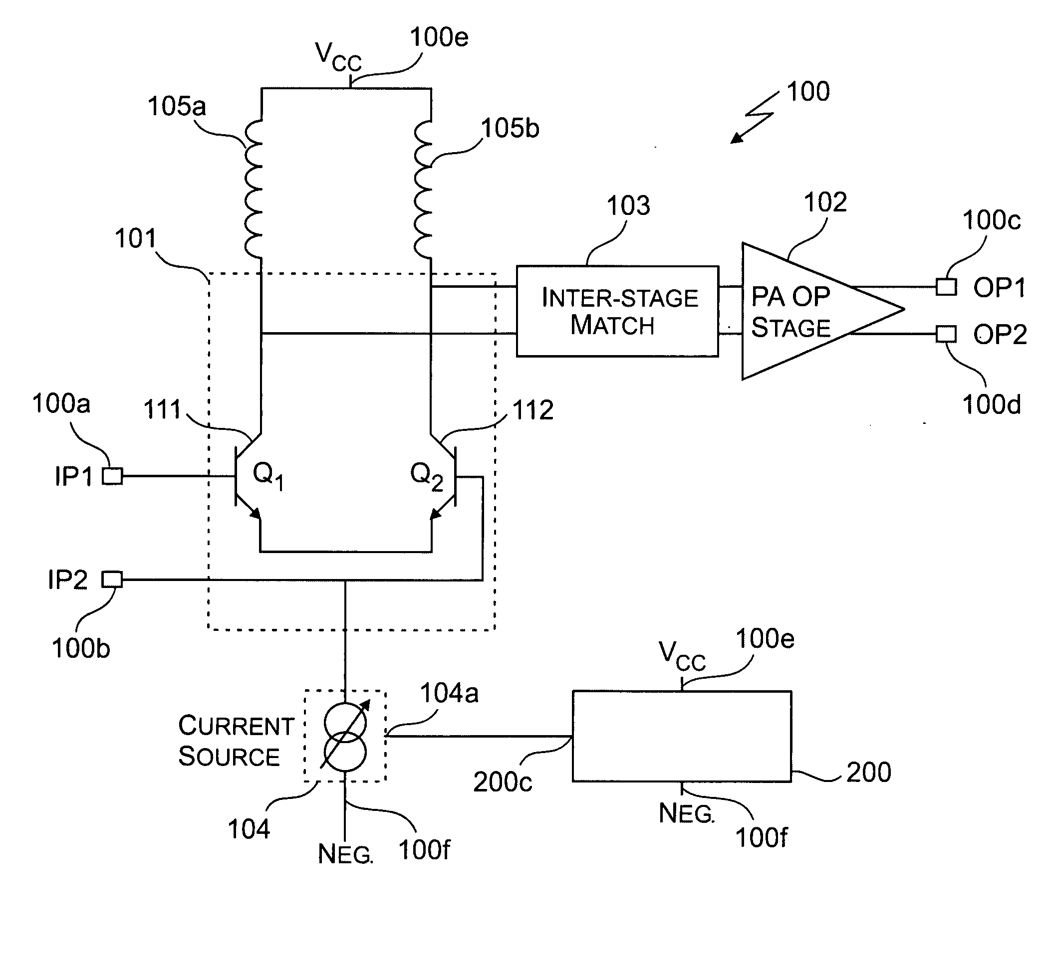
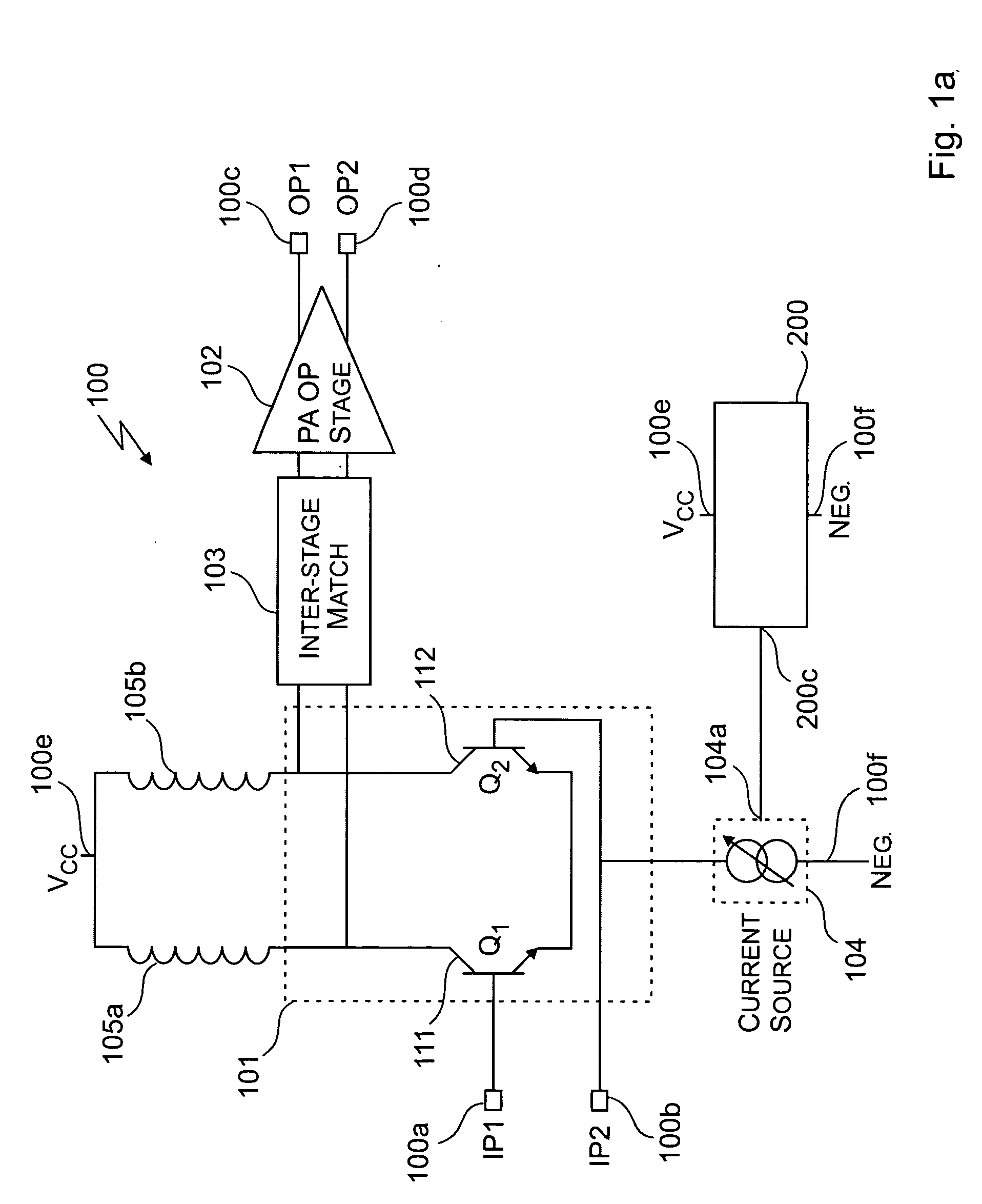
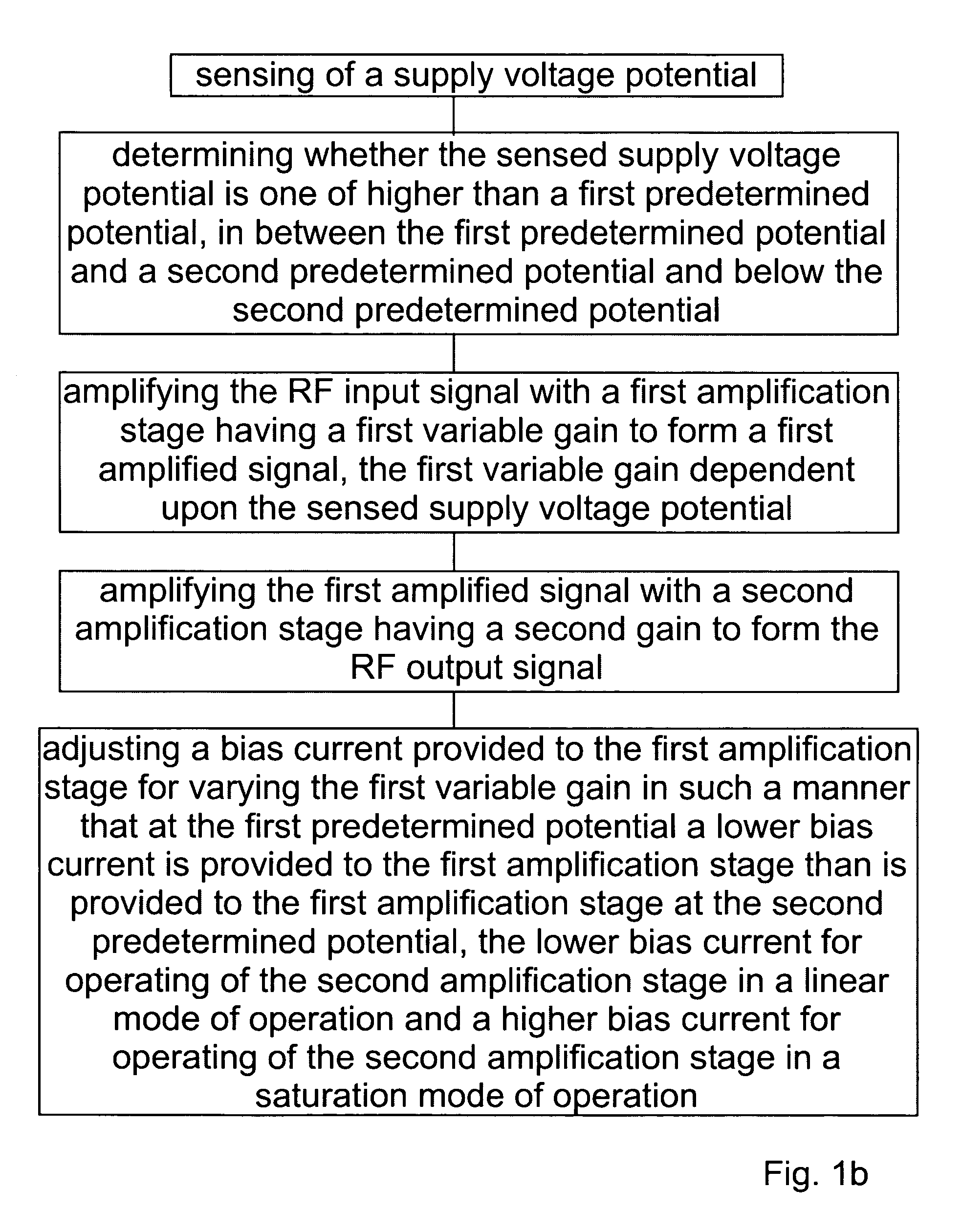
[0020] The primary focus of the embodiments of the invention is the control circuit 200 (FIG. 2a) and control circuit 220 (FIG. 2b) and their use in controlling of the controllable current source 104. FIG. 2a illustrates the control circuit 200 in accordance with the invention. The control circuit 200 is comprised of the following circuit blocks: a supply voltage sense circuit 201, a first multiplier circuit 202, a bandgap reference circuit 203, and a current summing circuit 204.

[0021] The supply voltage sense circuit 201 has a first input port connected to the first supply voltage input port 100e for sensing a potential of the first supply voltage (Vcc) applied thereto relative to a reference voltage from a reference source (not shown) provided to a second input port thereof. An output port of the supply voltage sense circuit 201 is used for providing a sense signal (Isense) (302FIG. 3a) to a first input port of a first multiplier circuit (M1) 202. Preferably M1202 is in the form o...

third embodiment

[0028]FIG. 2b illustrates the control circuit 220 in accordance with the invention. The control circuit 220 includes the circuitry of control circuit 200, but further comprises a second multiplier circuit 205, a charge pump and ramp control circuit 206 and an integrating capacitor 207. The second multiplier circuit 205 has a first input port, a second input port and an output port. Preferably the second multiplier circuit 205 is an analog multiplier circuit, preferably in the form of a Gilbert gain cell. The summed current provided from the output port of the current summing circuit 204 is provided to the first input port of the second multiplier circuit 205. The output port of M2 is directly connected to the output port 200c of the control circuit. An output signal from the second multiplier circuit 205 serves as the control signal (Icontrol) that is provided to the control port 104a of the controllable current source 104 used for biasing of transistors Q1111 and Q2112 (FIG. 1). Th...


PUM


Abstract

A power amplifier circuit is disclosed having a first amplification stage and a second amplification stage. The first amplification stage is biased using a controllable current source that provides a variable bias current thereto. A control circuit is provided for controlling the variable bias current in dependence upon the supply voltage and temperature of the power amplifier circuit. The control signal varies the variable bias current in dependence upon the supply voltage varying between first and second potential, where each potential supplies sufficient potential for operation of the power amplifier circuit.

Description

FIELD OF THE INVENTION [0001] The invention relates to the field of power amplifier circuits and more specifically to the field of controlling of amplification stages forming a power amplifier in order to attain a predetermined range of output signal power. BACKGROUND OF THE INVENTION [0002] For many applications, Radio Frequency (RF) Power Amplifiers (PAs) are required to have an output signal power that is independent of PA supply voltage and PA operating temperature. [0003] Prior art PA circuits generally have a first stage that is supplied with a ramped voltage supply that is used to control an output signal of the first stage in a controllable manner. Unfortunately, a disadvantage of the old technology is that fine control for controlling of amplitude of the output signal is not easily attained. A collector emitter saturation voltage of the first stage RF transistor, or transistors, limits the first stage output signal. At saturation, the amplitude of the output signal is hard ...

Claims


Application Information

Patent Timeline
Patent Type & Authority Applications(United States)
IPC IPC(8): H03F3/00H03F3/189H03F3/45
CPCH03F3/45085H03F2203/45456H03F2203/45682H03F2203/45638H03F2203/45466
Inventor WHITTAKER, EDWARD J.W.ZELLEY, CHRISTOPHER A.
Owner SIGE SEMICON
Why Eureka
Try Eureka