Magnetoresistance effect element, its manufacturing method, magnetic reproducing element and magnetic memory

a technology of magnetoresistance effect and element, applied in the field of magnetoresistance effect (mr) elements, can solve the problems of increasing the difficulty of ensuring sufficient signal intensity, almost impossible to realize a practical magnetoresistance effect element, and difficult control of the magnetic domain structure and the configuration of the point conta

Inactive Publication Date: 2005-05-05
KK TOSHIBA
View PDF11 Cites 35 Cited by
  • Summary
  • Abstract
  • Description
  • Claims
  • Application Information

AI Technical Summary

Problems solved by technology

In the technical field of magnetic recording, enhancement of the recording density inevitably requires miniaturization of the recording bit, and this makes it more and more difficult to ensure sufficient signal intensity.
These magnetic nanocontacts also exhibit a large mangetoresistance change, however, the strucutre of these magnetic nanocontacts makes it almost impossible to realize a practical magnetoresistance effect element.
However, it is difficult to control the magnetic domain structure and the configuration of the point contact, therefore, the resulting magnetoresistance ratio is as small as 14% or even smaller.
Magnetic nanocontacts have a potential to exhibit a large magnetoresistance ratio, however, in order to ensure a large magnetoresistive effect therewith, the structures proposed by the above-noted articles include placing two needle-shaped ferromagnetic elements in tip-to-tip abutment or growing a micro column between two wires by an electroplating technique, and this and other requirements make it difficult to accurately control the contact portions in the manufacturing process.

Method used


Image

  • Magnetoresistance effect element, its manufacturing method, magnetic reproducing element and magnetic memory
  • Magnetoresistance effect element, its manufacturing method, magnetic reproducing element and magnetic memory
  • Magnetoresistance effect element, its manufacturing method, magnetic reproducing element and magnetic memory

Examples


examples

[0182] Herein below, embodiments of the invention will be explained in greater detail in conjunction with examples.

first example

[0183] As the first example of the invention, there is a model of magnetoresistance effect element a magnetic nanocontact on nickel (Ni) covered by alumina.

[0184] First of all, for obtaining the multi-layered structure shown in FIG. 8A, aluminum (Al) was deposited by vapor deposition on a ferromagnetic layer 1 made of nickel, and its top surface was oxidized to form alumina as an insulating layer.

[0185] After that, a needle 110 coated with conductive diamond and used to form a micro through hole was driven close to the top surface of alumina as shown in FIG. 8B. Then, the voltage of 0.01 V was applied across the nickel layer 1 and the needle 110, and while monitoring the flowing current, the needle 110 was driven into the alumina insulating layer 3. Movement of the needle 110 was controlled by making use of thermal expansion caused by electric heating of a distance-changing functional portion 130A attached to an upper portion of the arm 140.

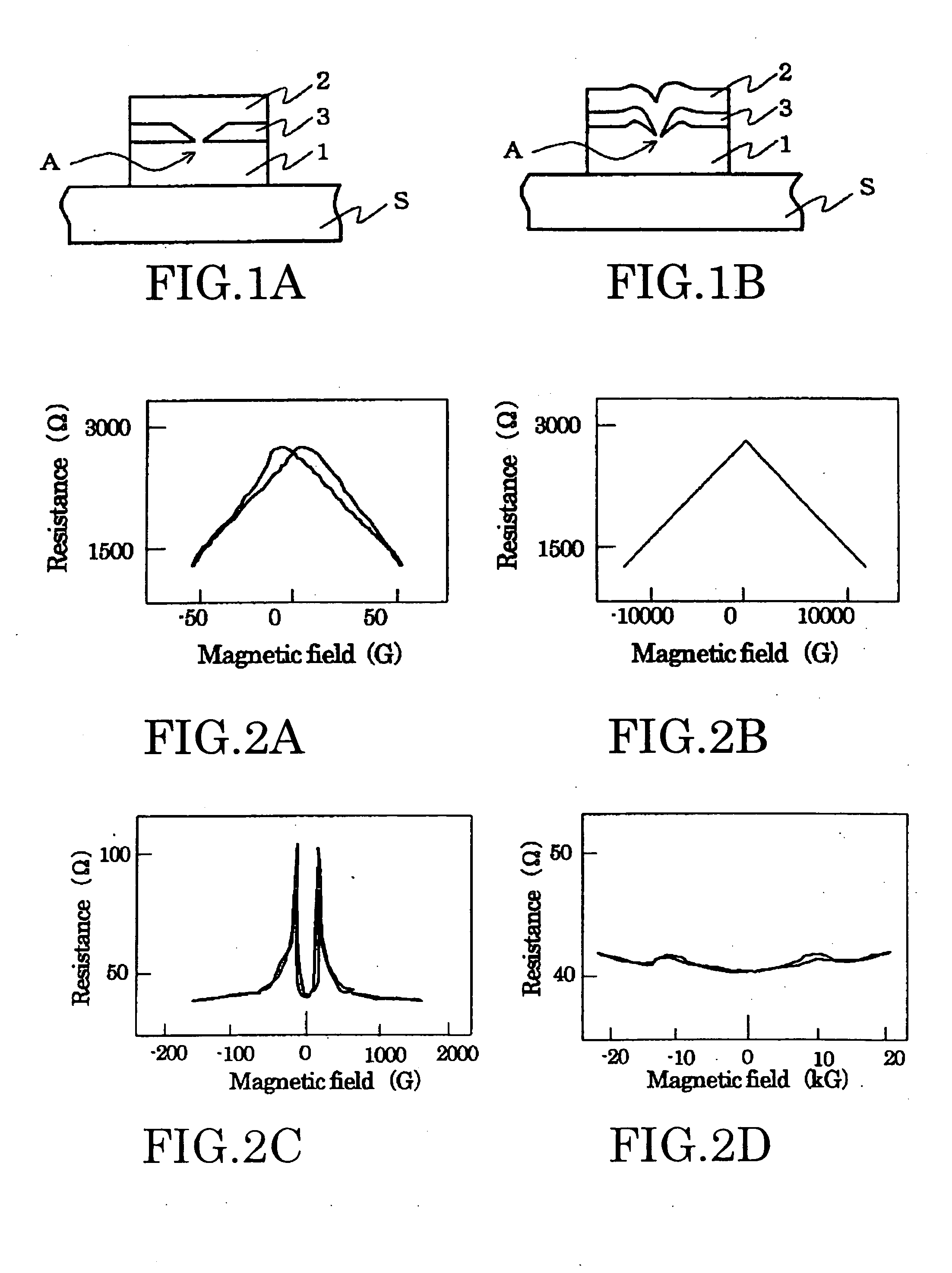
[0186]FIGS. 17A and 17B are graph diagr...

second example

[0190] As the second example of the invention, a reproducing element for magnetic recording was prepared by using the manufacturing method used in the first embodiment explained above.

[0191] That is, a thick cobalt (Co) film was formed on the substrate, and alumina was formed thereon. Then, after making the micro through hole A, 20 nm thick Permalloy was deposited by vapor deposition. Part of the Permalloy above the micro through hole A was patterned into an approximately 20×20 nm square, and part of the underlying cobalt layer as large as 100 nm was cut out. A conductive wire was provided thereto, and the magnetoresistance effect element was moved on the surface of the vertically magnetized medium. As a result, a change of resistance corresponding to the change of the medium signal was observed.


PUM

PropertyMeasurementUnit
widthaaaaaaaaaa
sizeaaaaaaaaaa
widthaaaaaaaaaa

Abstract

A magnetoresistance effect element includes a first ferromagnetic layer (1), insulating layer (3) overlying the first ferromagnetic layer, and second ferromagnetic layer (2) overlying the insulating layer. The insulating layer has formed a through hole (A) having an opening width not larger than 20 nm, and the first and second ferromagnetic layers are connected to each other via the through hole.

Description

CROSS-REFERENCE TO RELATED APPLICATIONS [0001] This application is based upon and claims the benefit of priority from the prior Japanese Patent Application No. 2001-284467, filed on Sep. 19, 2001; the entire contents of which are incorporated herein by reference. BACKGROUND OF THE INVENTION [0002] This invention relates to a magnetoresistance effect (MR) element, its manufacturing method, and its use as a magnetic recording element or a magnetic memory. More particularly, the invention relates to a magnetoresistance effect element having magnetic nanocontacts that exhibit high magnetoresistance ratios, its manufacturing method, and its use as a magnetic reproducing element or a magnetic memory. [0003] Since the discovery that a giant magnetoresistance effect occurs when a current is supplied to flow in parallel with the major plane of a multi-layered structure, efforts have been made to find systems having still larger magnetoresistance ratios. Thus, ferromagnetic tunnel junction el...

Claims


Application Information

Patent Timeline
Patent Type & Authority Applications(United States)
IPC IPC(8): B32B7/02G11B5/39
CPCB32B7/02Y10T29/49043B82Y25/00G01R33/093G11B5/39G11B5/3929G11B2005/3996G11C11/16H01L43/08H01L43/12Y10T428/1143Y10T29/49044Y10T428/12931Y10T428/1114Y10T428/12465Y10T428/325Y10T428/12986B82Y10/00G11C11/161H10N50/01H10N50/10
Inventor OKUNO, SHIHOOHSAWA, YUICHIHANEDA, SHIGERUKAMIGUCHI, YUZOKISHI, TATSUYA
Owner KK TOSHIBA
Why Eureka
Try Eureka