Triple-gate mosfet transistor and methods for fabricating the same

a mosfet transistor and triple-gate technology, applied in the field of mosfet transistors, can solve the problems of increasing off-state current, limiting the extent to which the dimensions of conventional planar transistors can be reliably scaled, and performance limitations are also a barrier to scaling conventional planar transistor dimensions, so as to reduce the effect of short channel effects, avoiding or reducing adverse effects of etched channel surfaces

Active Publication Date: 2005-05-05
TEXAS INSTR INC
View PDF6 Cites 9 Cited by
  • Summary
  • Abstract
  • Description
  • Claims
  • Application Information

AI Technical Summary

Problems solved by technology

However, lithography generally limits the extent to which transistor dimensions can be reliably scaled, wherein the minimum gate length is typically limited to the smallest dimension that can be reliably and repeatably patterned and etched using current photolithographic and etching techniques.
In addition to fabrication process limitations, performance limitations are also a barrier to scaling conventional planar transistor dimensions, particularly the gate length.
In shorter channel devices, however, the channel region is also affected by the source and drain voltages, leading to increased off-state current due to Vt roll off, degraded subthreshold slope, and degraded output current.
In practice, however, the conventional multi-gate approaches have suffered from cost and performance shortcomings, because SOI wafers are more expensive than ordinary silicon substrates and because the channel surface has been etched while carving the upper SOI silicon layer into islands or blocks.

Method used


Image

  • Triple-gate mosfet transistor and methods for fabricating the same
  • Triple-gate mosfet transistor and methods for fabricating the same
  • Triple-gate mosfet transistor and methods for fabricating the same

Examples


Embodiment Construction

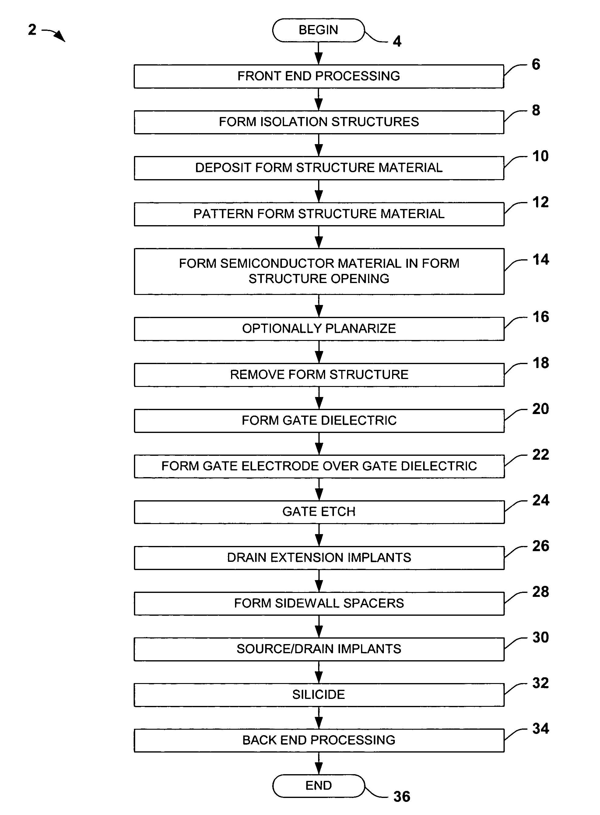
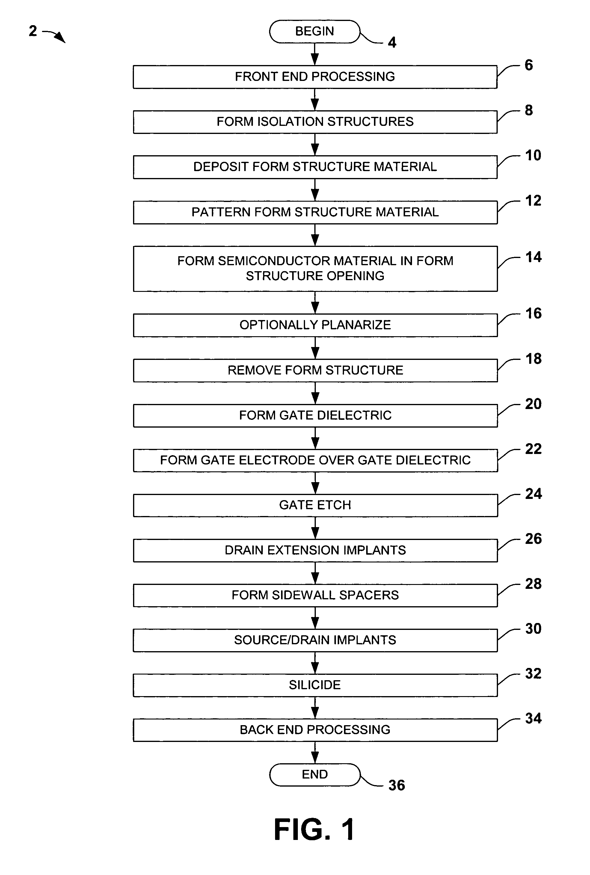
[0015] The present invention will now be described with reference to the attached drawing figures, wherein like reference numerals are used to refer to like elements throughout, and wherein the illustrated structures are not necessarily drawn to scale. The invention relates to transistor devices and fabrication methods wherein a semiconductor body is over a starting structure to allow multi-gate device fabrication using standard semiconductor wafers or other starting structures. In one example, illustrated and described below, the semiconductor body is formed in a cavity of a temporary form structure, through deposition of epitaxial silicon or other semiconductor material, after which the form structure is removed. The formed semiconductor body includes a single generally planar bottom surface situated over the starting material and has three body portions, two of which are doped to form source / drains, with the other body portion forming a transistor channel between the doped source...


PUM


Abstract

Fabrication methods are presented in which a semiconductor body is deposited in a cavity of a temporary form structure above a semiconductor starting structure. The formed semiconductor body can be epitaxial silicon deposited in the form cavity over a silicon substrate, and includes three body portions, two of which are doped to form source / drains, and the other forming a transistor channel that overlies the starting structure. A gate structure is formed along one or more sides of the channel body portion to create a MOS transistor.

Description

RELATED APPLICATIONS [0001] This application is related to U.S. patent application Ser. No. ______ (Attorney Docket No. TI-36030), filed on ______, entitled MULTIPLE-GATE MOSFET DEVICE WITH LITHOGRAPHY INDEPENDENT SILICON BODY THICKNESS AND METHODS FOR FABRICATING THE SAME.FIELD OF INVENTION [0002] The present invention relates generally to semiconductor devices and more particularly to multi-gate MOSFET transistors and fabrication methods therefor. BACKGROUND OF THE INVENTION [0003] Metal-oxide-semiconductor field-effect transistors (MOSFETs) are widely used in the electronics industry for switching, amplification, filtering, and other tasks related to both analog and digital electrical signals. Conventional planar MOS transistors include a gate dielectric overlying a channel region at the upper surface of a silicon substrate and a gate electrode situated above the gate dielectric. Source and drain regions are formed in the substrate on either lateral side of the channel. In operat...

Claims


Application Information

Patent Timeline
Patent Type & Authority Applications(United States)
IPC IPC(8): H01L21/00H01L21/336H01L29/76H01L29/78
CPCH01L29/665H01L29/7833H01L29/66795H01L29/6659
Inventor CHAMBERS, JAMES JOSEPHVISOKAY, MARK ROBERT
Owner TEXAS INSTR INC
Why Eureka
Try Eureka