Non-volatile memory and manufacturing method using STI trench implantation

a manufacturing method and non-volatile memory technology, applied in the field of non-volatile memory, can solve the problems of reducing design features, challenging the limitations of conventional semiconductor technology, and non-functional areas, and achieve the effect of reducing device size and compact dimensions

Inactive Publication Date: 2005-05-12
CHARTERED SEMICONDUCTOR MANUFACTURING
View PDF5 Cites 9 Cited by
  • Summary
  • Abstract
  • Description
  • Claims
  • Application Information

AI Technical Summary

Benefits of technology

[0011] The present invention provides a method for manufacturing an integrated circuit structure. A semiconductor substrate is provided, and two trenches are formed in the semiconductor substrate to define an active region therebetween. An implanted source region is formed in one of the trenches on one side of the active region. An implanted drain region is formed in the other trench on the other side of the active region. Shallow trench isolations are then formed in the trenches. One or more gates are formed over the active region, and contacts to the implanted source region and the implanted drain region are formed. This method produces a flash memory device with smaller memory cells having more compact dimensions, resulting in the reduction of device size.

Problems solved by technology

The continuing reduction of design features, however, generates numerous problems challenging the limitations of conventional semiconductor technology.
One challenge in miniaturization is presented by the so-called “isolation structures” that are necessary to prevent each memory cell from interfering with the operation of its neighbors.
One problem with the LOCOS structure is that the structure includes non-functional areas that waste valuable space on the semiconductor substrate, interfering with the need to achieve denser and denser packing.
However, STI structures are often not used in flash memory due to the difficulty in forming the source line that connects the cells in each row.
The increased electrical resistance reduces the operational performance of the memory.
Unfortunately, these interconnecting conductors must sometimes be positioned farther apart than desirable for the device elements to which they are connected.
Solutions to these problems have been long sought but prior developments have not taught or suggested any solutions and, thus, solutions to these problems have long eluded those skilled in the art.

Method used


Image

  • Non-volatile memory and manufacturing method using STI trench implantation
  • Non-volatile memory and manufacturing method using STI trench implantation
  • Non-volatile memory and manufacturing method using STI trench implantation

Examples


Embodiment Construction

[0024] The term “horizontal” as used herein is defined as a plane parallel to the conventional plane or surface of a silicon wafer, regardless of its orientation. The term “vertical” refers to a direction perpendicular to the horizontal as just defined. Terms, such as “on”, “above”, “below”, “bottom”, “top”, “side” (as in “sidewall”), “higher”, “lower”, “over”, and “under”, are defined with respect to the horizontal plane.

[0025] The term “processing” as used herein includes deposition of material or photoresist, patterning, exposure, development, etching, cleaning, and / or removal of the material or photoresist as required in forming a described structure.

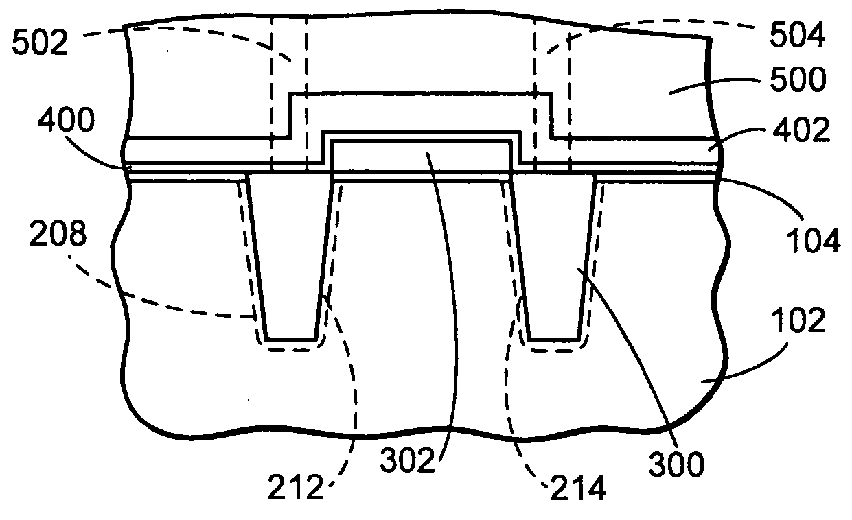
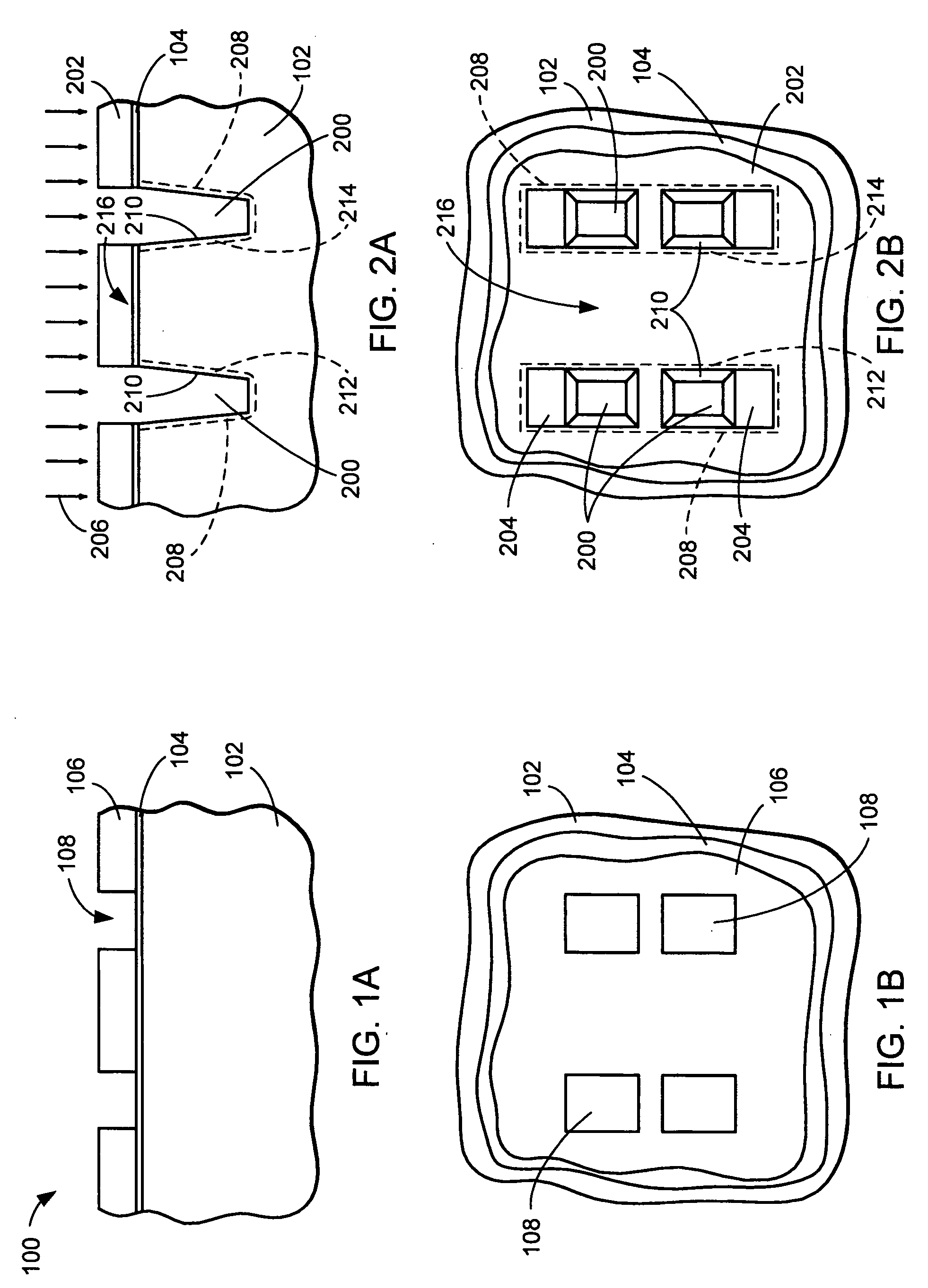
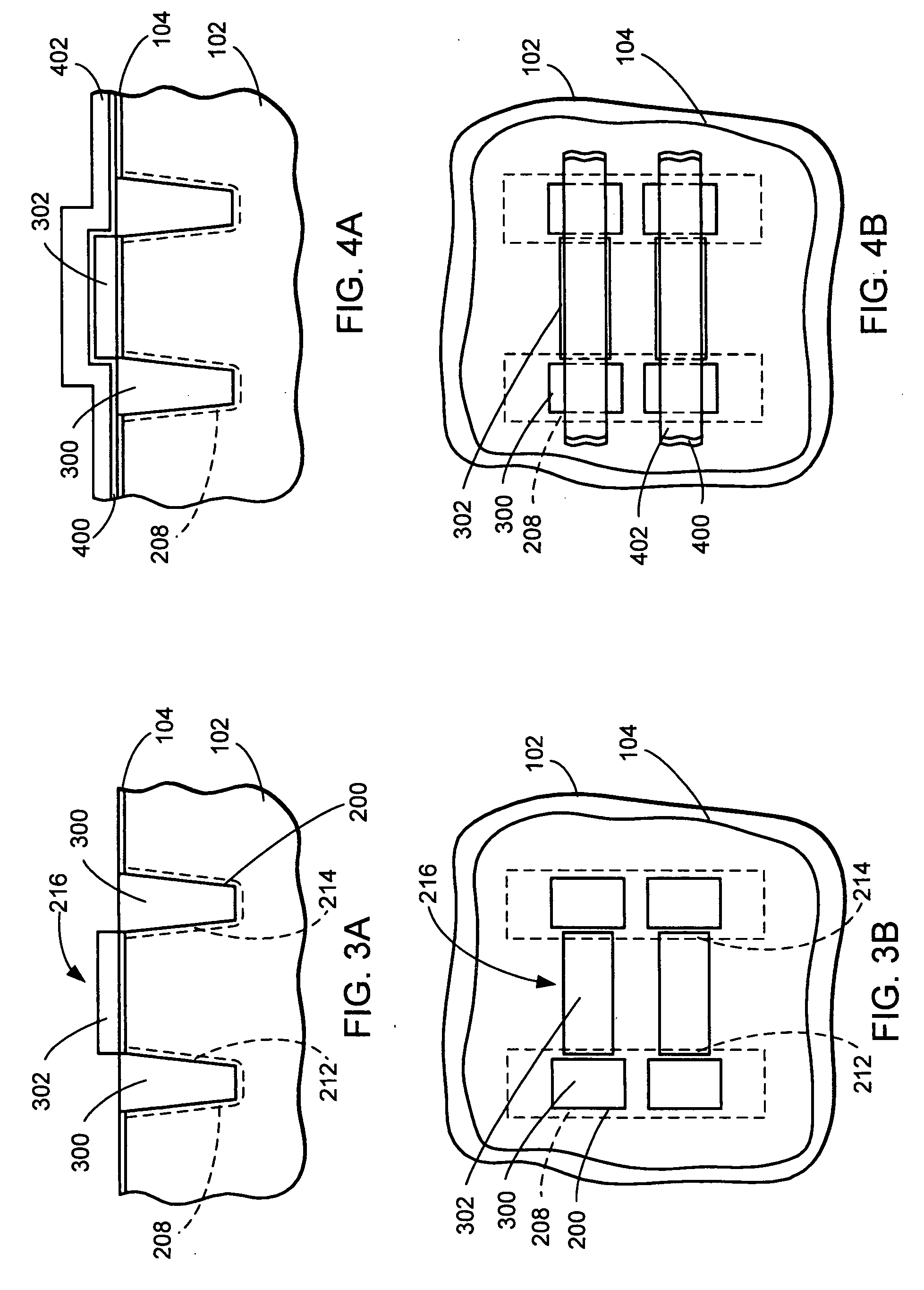
[0026] Typical prior art methods for fabricating non-volatile memory cells employ shallow trench isolations (“STI”s) to define the device active area. The defining element of the non-volatile memory cell is the presence of a floating gate. A very thin tunneling oxide layer overlies the semiconductor substrate. The floating gate is...


PUM


Abstract

A method for manufacturing an integrated circuit structure includes providing a semiconductor substrate and forming two trenches in the semiconductor substrate to define an active region therebetween. An implanted source region is formed in one of the trenches on one side of the active region. An implanted drain region is formed in the other trench on the other side of the active region. Shallow trench isolations are then formed in the trenches. One or more gates are formed over the active region, and contacts to the implanted source region and the implanted drain region are formed.

Description

TECHNICAL FIELD [0001] The present invention relates generally to semiconductor devices and methods for the manufacturing thereof, and more specifically to non-volatile memories. BACKGROUND ART [0002] Electronic equipment, such as televisions, telephones, radios, and computers, is constructed using semiconductor microprocessors, integrated circuits, memory chips, and the like. These semiconductor components are typically fabricated on a semiconductor substrate and are constructed using various microelectronic devices such as transistors, capacitors, diodes, resistors, and so forth. Each microelectronic device is typically a pattern of conductor, semiconductor, and insulator regions formed on the semiconductor substrate. [0003] Conventional semiconductor memory devices fall into two general classes: volatile memories and non-volatile memories. Volatile memories are generally faster and less expensive, but lose (or “forget”) their data when the power is turned off. Non-volatile memori...

Claims


Application Information

Patent Timeline
Patent Type & Authority Applications(United States)
IPC IPC(8): H01L21/336H01L21/762H01L21/8247H01L27/115
CPCH01L21/76237H01L29/66825H01L27/11521H01L27/115H10B69/00H10B41/30
Inventor CHAN, TZE HO SIMONLI, WEININGQUEK, ELGINZHENG, JIA ZHENYELEHANKA, PRADEEP RAMACHANDRAMURTHYLAI, TOMMY
Owner CHARTERED SEMICONDUCTOR MANUFACTURING
Why Eureka
Try Eureka