Method for integrating a high-k gate dielectric in a transistor fabrication process

a fabrication process and dielectric technology, applied in the field of semiconductor devices, can solve problems such as high tunneling current, low efficiency, and low reliability of fets

Inactive Publication Date: 2005-05-12
GLOBALFOUNDRIES INC
View PDF16 Cites 29 Cited by
  • Summary
  • Abstract
  • Description
  • Claims
  • Application Information

AI Technical Summary

Benefits of technology

[0005] The present invention addresses and resolves the need in the art for an effective method for integrating a high-k gate dielectric in a transistor fabrication process.

Problems solved by technology

High-k gate dielectrics are desirable in small feature size technologies since conventional gate dielectrics, such as silicon dioxide, are too thin and they result in high tunneling current, as well as other problems, which decrease performance and reliability of FETs.
However, problems can occur during integration of a high-k gate dielectric into a transistor fabrication process.
However, during the plasma etch, the plasma can damage the sidewalls of the gate stack, including exposed portions of gate electrode and high-k dielectric segments.
For example, the plasma can etch away a portion of the high-k dielectric material and can damage the chemical structure of the high-k dielectric.
However, the wet clean process can also damage the high-k dielectric by stripping off some of the high-k dielectric material.
Additionally, oxygen can laterally diffuse into the high-k gate dielectric during subsequent process steps and alter the properties of the high-k dielectric material and the transistor gate.

Method used


Image

  • Method for integrating a high-k gate dielectric in a transistor fabrication process
  • Method for integrating a high-k gate dielectric in a transistor fabrication process
  • Method for integrating a high-k gate dielectric in a transistor fabrication process

Examples


Embodiment Construction

[0010] The present invention is directed to method for integrating a high-k gate dielectric in a transistor fabrication process. The following description contains specific information pertaining to the implementation of the present invention. One skilled in the art will recognize that the present invention may be implemented in a manner different from that specifically discussed in the present application. Moreover, some of the specific details of the invention are not discussed in order not to obscure the invention.

[0011] The drawings in the present application and their accompanying detailed description are directed to merely exemplary embodiments of the invention. To maintain brevity, other embodiments of the present invention are not specifically described in the present application and are not specifically illustrated by the present drawings.

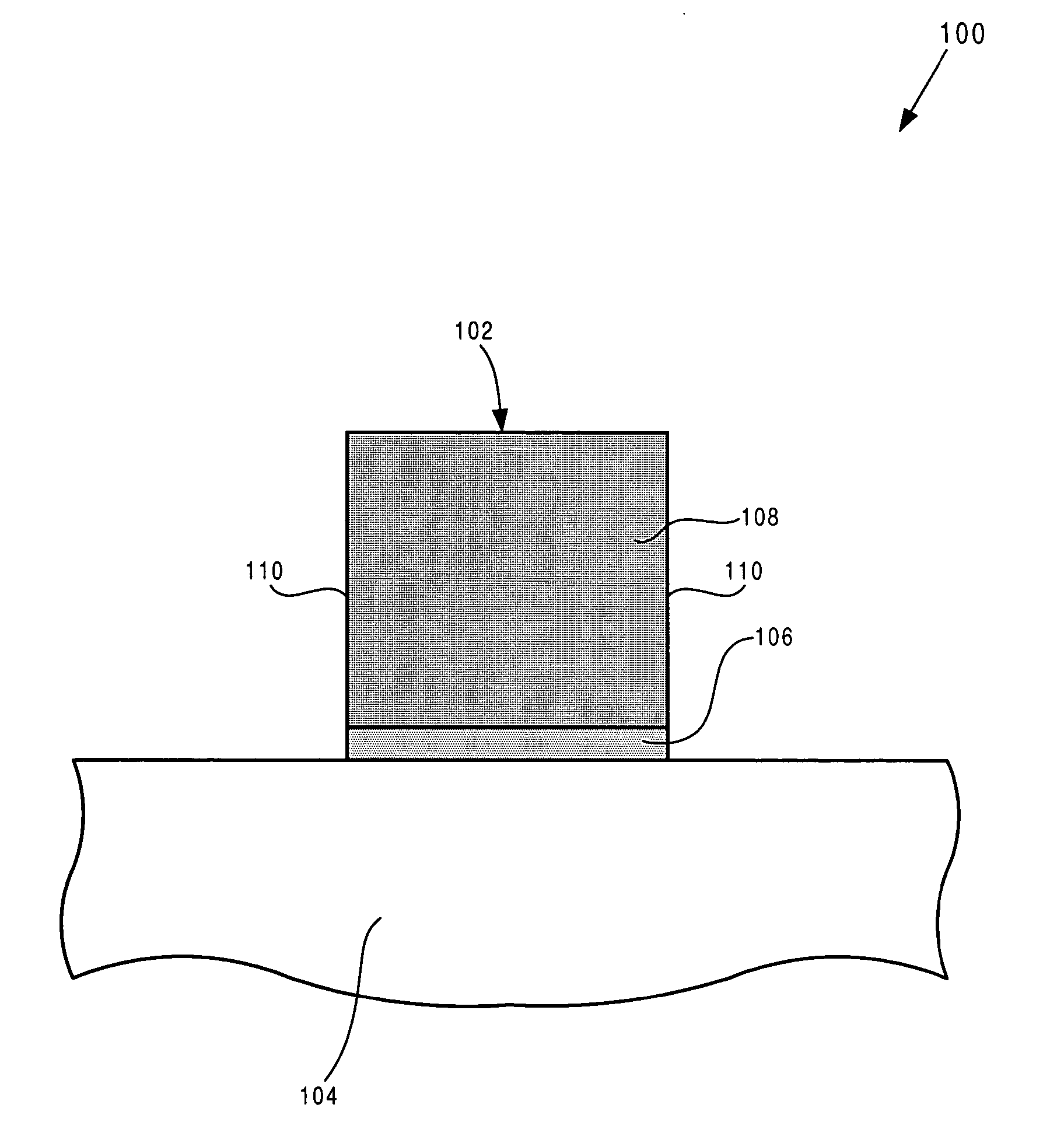
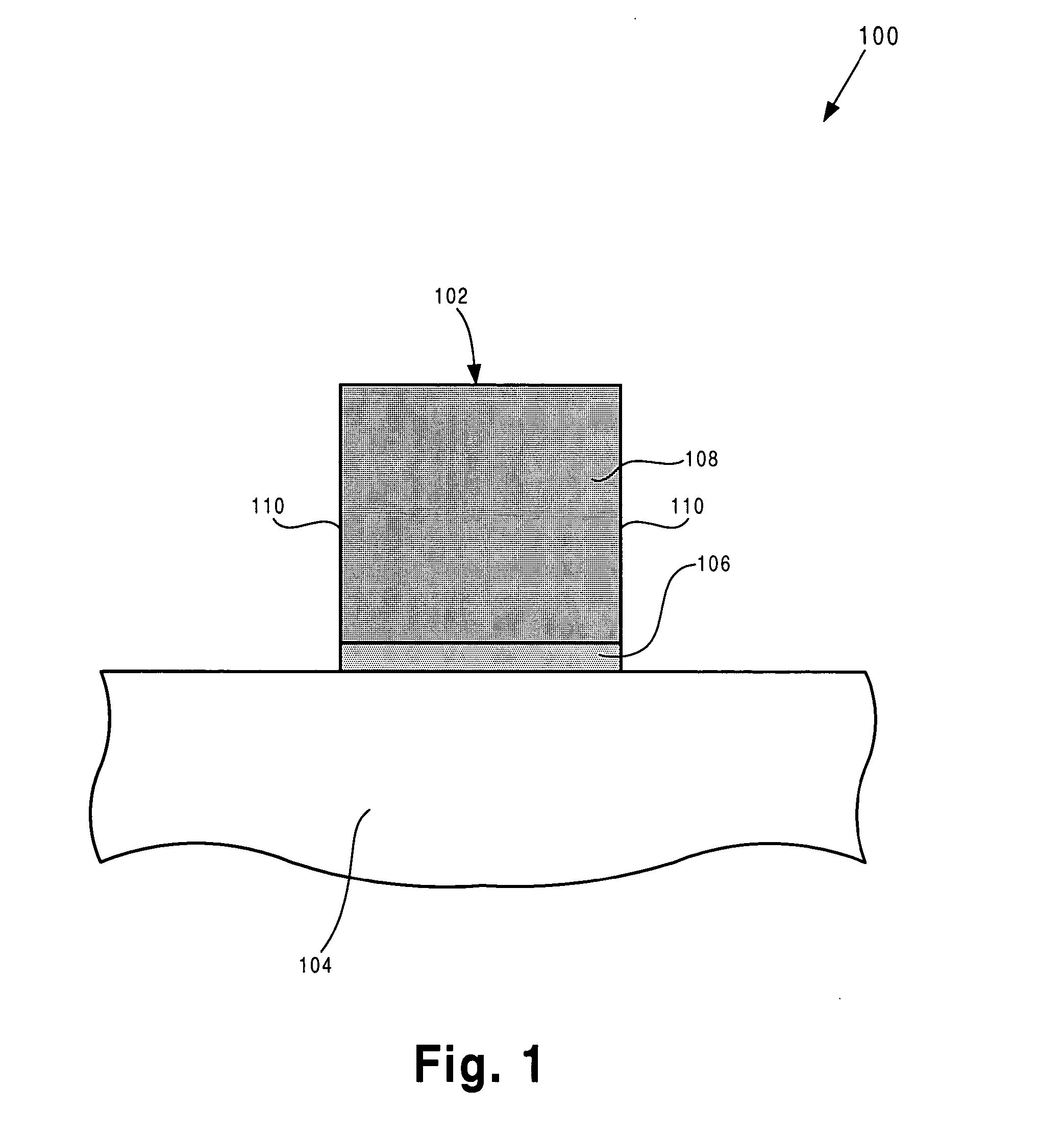
[0012]FIG. 1 shows a cross-sectional view of an exemplary structure including an exemplary gate stack in accordance with one embodiment...


PUM


Abstract

According to one exemplary embodiment, a method for forming a field-effect transistor on a substrate, where the substrate includes a high-k dielectric layer situated over the substrate and a gate electrode layer situated over the high-k dielectric layer, comprises a step of etching the gate electrode layer and the high-k dielectric layer to form a gate stack, where the gate stack comprises a high-k dielectric segment situated over the substrate and a gate electrode segment situated over the high-k dielectric segment. According to this exemplary embodiment, the method further comprises performing a nitridation process on the gate stack. The nitridation process can be performed by, for example, utilizing a plasma to nitridate sidewalls of the gate stack, where the plasma comprises nitrogen. The nitridation process can cause nitrogen to enter the high-k dielectric segment and form an oxygen diffusion barrier in the high-k dielectric segment, for example.

Description

TECHNICAL FIELD [0001] The present invention is generally in the field of semiconductor devices. More particularly, the present invention is in the field of fabrication of field effect transistors. BACKGROUND ART [0002] As field effect transistors (“FET”), such as PFETs and NFETs, are scaled down in size, semiconductor manufactures have utilized gate dielectrics having a high dielectric constant (“high-k”) to improve FET performance and reliability. High-k gate dielectrics are desirable in small feature size technologies since conventional gate dielectrics, such as silicon dioxide, are too thin and they result in high tunneling current, as well as other problems, which decrease performance and reliability of FETs. However, problems can occur during integration of a high-k gate dielectric into a transistor fabrication process. [0003] In a conventional transistor fabrication process incorporating a high-k gate dielectric, a gate stack can be formed by etching a gate electrode layer an...

Claims


Application Information

Patent Timeline
Patent Type & Authority Applications(United States)
IPC IPC(8): H01L21/28H01L29/51
CPCH01L21/28176H01L21/28202H01L29/518H01L29/517H01L21/28247H01L21/02247H01L21/02252H01L29/511
Inventor LABELLE, CATHERINE B.ANG, BOON-YONGJEON, JOONG S.HOLBROOK, ALLISON K.XIANG, QIZHONG, HUICAI
Owner GLOBALFOUNDRIES INC
Why Eureka
Try Eureka