

Method and apparatus for crystal analysis
a crystal analysis and crystal technology, applied in the field of crystal analysis and crystal analysis apparatus, can solve the problems of difficult to have the resolution (ie., spatial resolution power) raised higher than the existing value, and the correlation between the two can not be easily identified, so as to achieve the effect of high resolution and eas
- Summary
- Abstract
- Description
- Claims
- Application Information
AI Technical Summary
Benefits of technology
Problems solved by technology
Method used
Image

Examples
Embodiment Construction
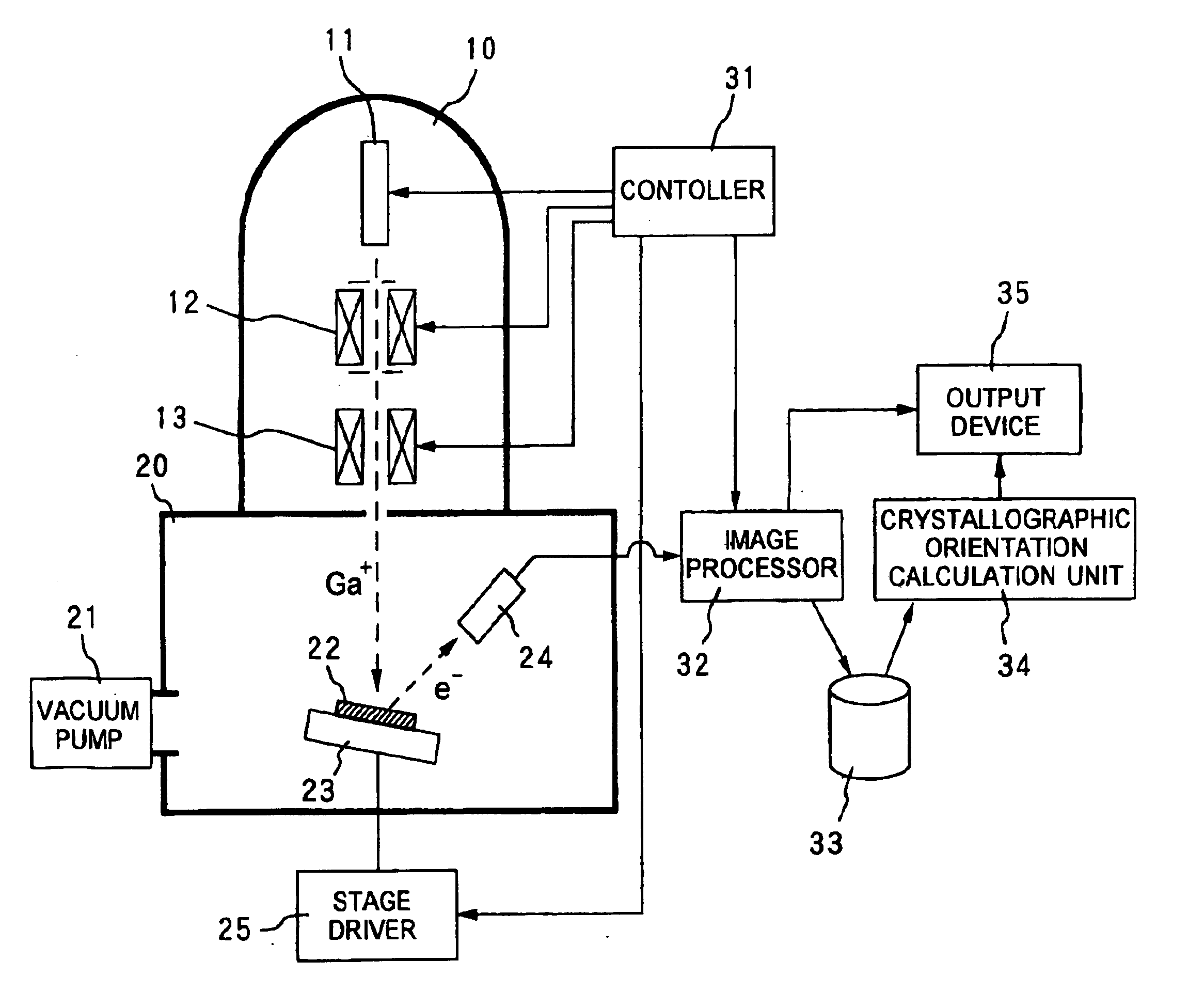
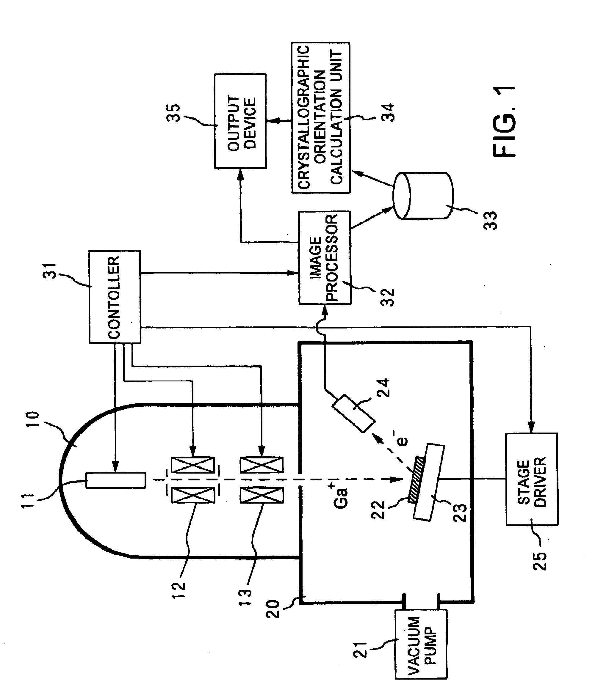
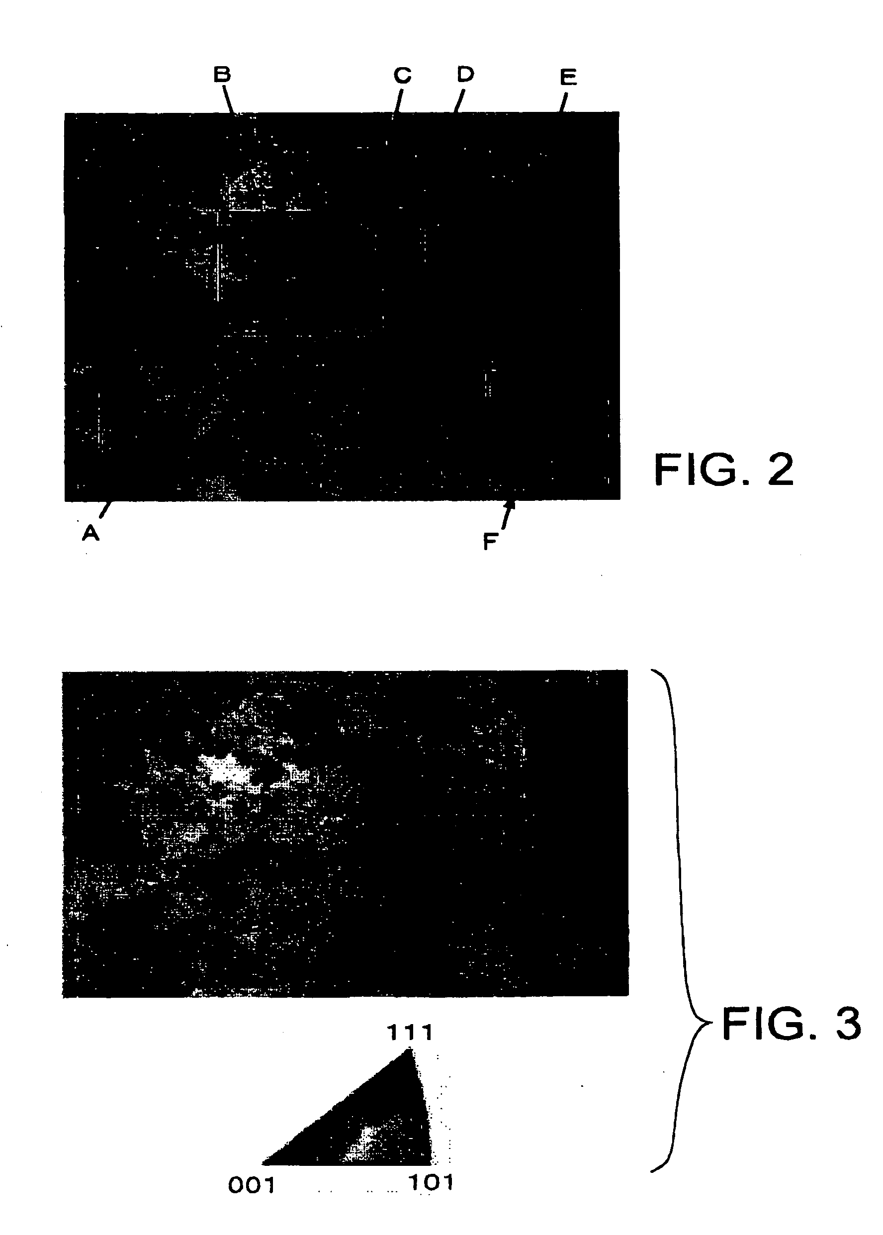
[0026] The method of crystal analysis according to the present invention is intended for analyzing the crystallographic orientations and crystal systems of a specimen surface based on the relation between the intensity of the secondary electron emitted from the specimen when the specimen surface is irradiated with an ion beam and the angle of incidence of the ion beam impinging on the specimen. It is possible to obtain the data that represent a two-dimensional distribution of the crystallographic orientations of crystal grains on a specimen surface by performing an observation by means of the scanning ion microscope while varying the incidence angle of the ion beam with respect to a specimen surface and analyzing a plurality of the scanning ion microscope images (hereinafter referred to as the SIM images) acquired at different incidence angles. This data representative of the two-dimensional distribution is equivalent to an inversion pole figure obtained by the measurements accordin...
PUM
 Abstract
Description
Claims
Application Information