Liquid crystal display panel
a liquid crystal display panel and display panel technology, applied in non-linear optics, instruments, optics, etc., can solve the problems of reducing the resolution of lcd, unable to achieve the reflection display panel of conventional transflective ips, and no such widening over the process limitation rule, etc., to achieve wide viewing angle, reduce interference, and high picture quality
- Summary
- Abstract
- Description
- Claims
- Application Information
AI Technical Summary
Benefits of technology
Problems solved by technology
Method used
Image
Examples
first embodiment
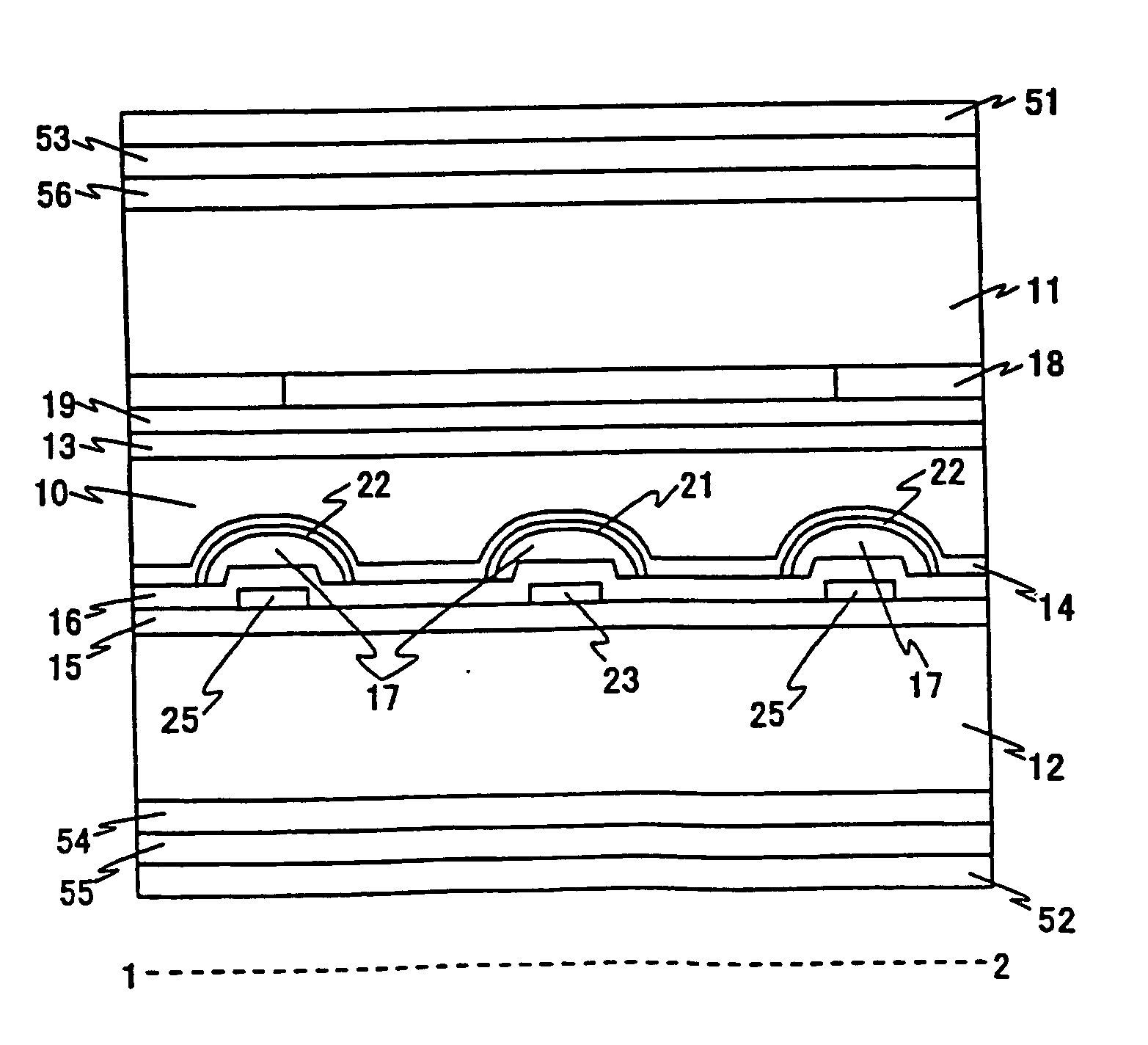
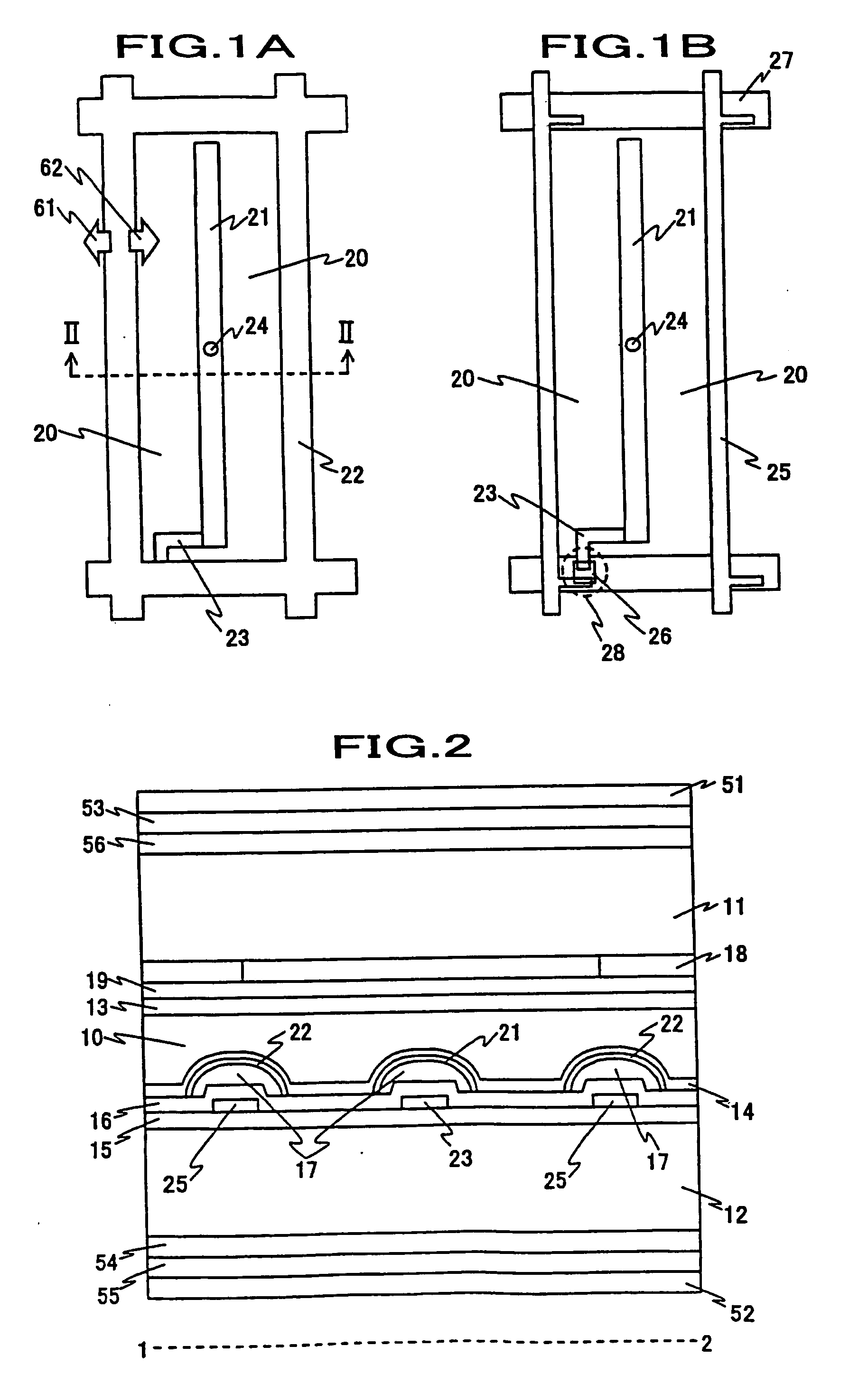
[0067] The cross sectional view of the present LCD panel is shown in FIG. 2 and the top view of the second substrate 12 is shown in FIG. 1. FIG. 2 shows a cut view in the dotted line II-II shown in FIG. 1 and the first substrate 11 and the second substrate 12 suspend the liquid crystal layer 10 therebetween. The first substrate 11 has an alignment layer 13, leveling layer 19 and the color filter 18 in the side adjacent to the liquid crystal layer 10.
[0068]FIG. 1A shows the pattern of the common electrode 22 on the second substrate 12 and FIG. 1B shows the layer pattern underneath the electrode 22. The second substrate 12 has the second alignment layer 13 in the side close to the liquid crystal layer 10 and has thin film transistor 28. The thin film transistor 28 has the construction of anti-stager and the channel is made of the amorphous silicon layer 26.
[0069] The scanning lines 27 and the signal lines 25 are crossing and the thin film transistor 28 locates thereon. The thin film...
second embodiment
[0104]FIG. 8 shows another embodiment of the present invention wherein the pixel electrode 21 and the common electrode 22 have the different cross sectional form by which the reflection characteristics are improved. The cross section of the pixel electrode 21 and the common electrode 22 is symmetry, which is same as the embodiment 1. The flat area is relatively reduced in comparison to the embodiment 1 and the slope area is increased.
[0105] The pixel electrode 21 and the common electrode 22 are made in the flowing method. The insulator 17 is patterned by using a grating mask which enables to progressively adjust exposure. The exposure is fully done onto the gaps between comb like electrodes and the insulation film is completely removed. The edge portions of the comb like electrodes 21 and 22 are incompletely exposed and rather thin insulation film is left. Since the central area of the comb like electrodes 21 and 22 is not exposed, the rather thick insulation film is left. The left...
third embodiment
[0108] As shown in FIG. 9, the cross section of the pixel electrode 21 and the common electrode 22 is formed in asymmetric. The decrease of the flat surface is same as the second embodiment but the flat portion is not on the central portion of the pixel electrode 21 and the common electrode 22.
[0109] The asymmetric cross section is formed in the following manufacturing process. By using grating mask as well as the second embodiment, the deviated portion on the comb like electrodes 21 and 22 is not exposed and thick insulation film is left. Other than this process, an additional organic insulating film is formed selectively to the central areas and the film is melted into the similar shape of the cross section.
[0110] According to the asymmetric shape of the cross section, higher rate of reflective scattering toward the normal direction for the incident lights from the slant direction of the one side of the cross section than the conventional LCD panel. The display even in the brigh...
PUM
 Abstract
Description
Claims
Application Information


